Preparation method of SOI wafer

A wafer and polysilicon technology, applied in the field of microelectronics, can solve the problems of difficult to produce materials with good thermal stability, low substrate surface resistivity, difficult to control, etc., so as to reduce the loss of the radio frequency substrate and reduce the parasitic surface. Conductivity, loss reduction effect

Pending Publication Date: 2020-01-31
SHENYANG SILICON TECH
View PDF0 Cites 0 Cited by
  • Summary
  • Abstract
  • Description
  • Claims
  • Application Information

AI Technical Summary

Problems solved by technology

(3) High-resistance SOI (Silicon-On-Insulator, silicon on insulating substrate) substrate: This type of substrate has structural advantages, but its performance is worse than that of the first type
One reason for the formation of a low-resistivity layer is: due to the possible presence of contaminants on the surface of the low-resistivity layer before bonding, during the bonding process these contaminants are encapsulated at the bonding interface and can diffuse to the high-resistivity substrate; Another reason for the low-resistance layer is that the content of oxygen atoms in the substrate is high, and heat treat

Method used


Image

  • Preparation method of SOI wafer
  • Preparation method of SOI wafer
  • Preparation method of SOI wafer

Examples


Embodiment 1

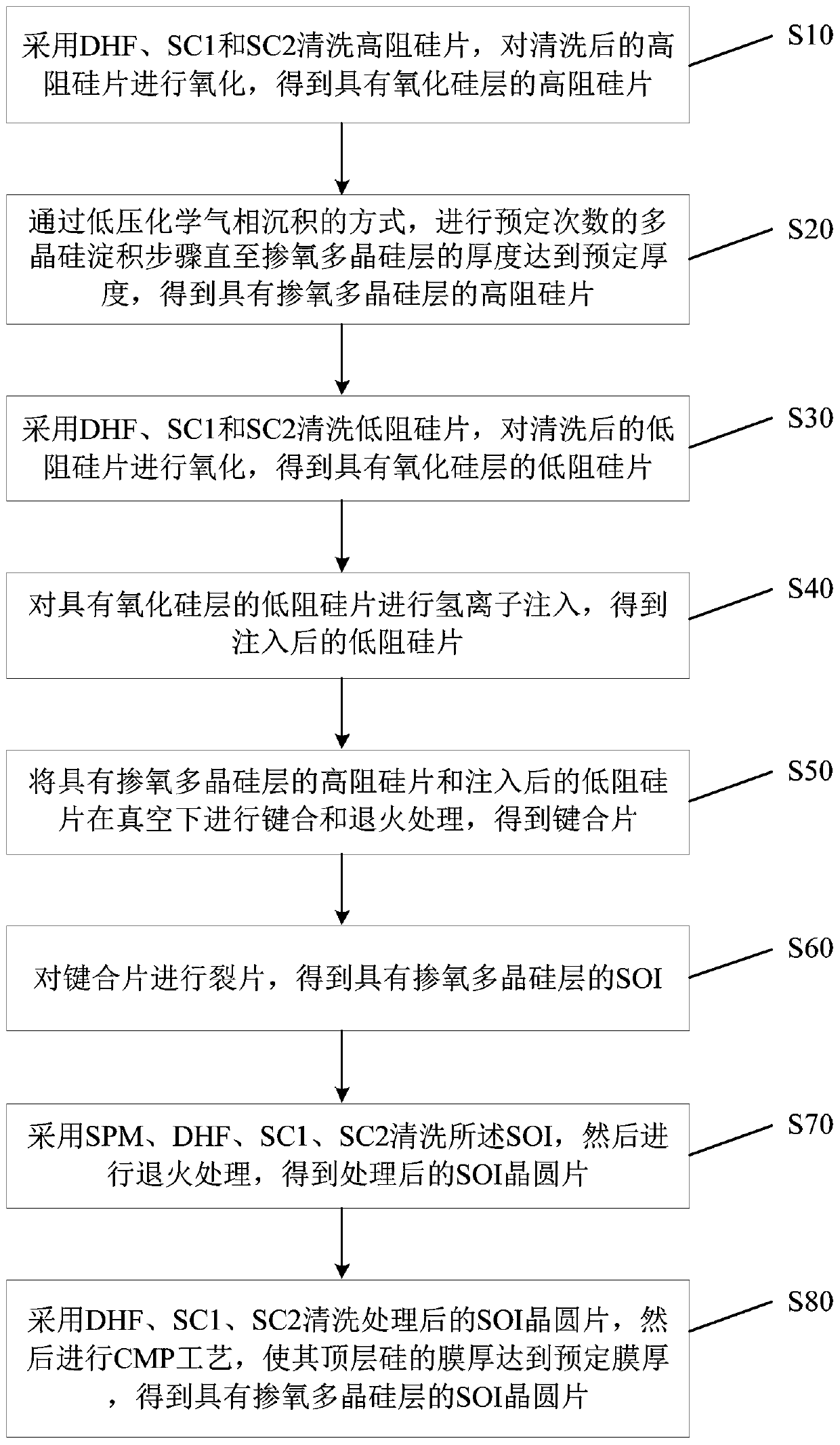
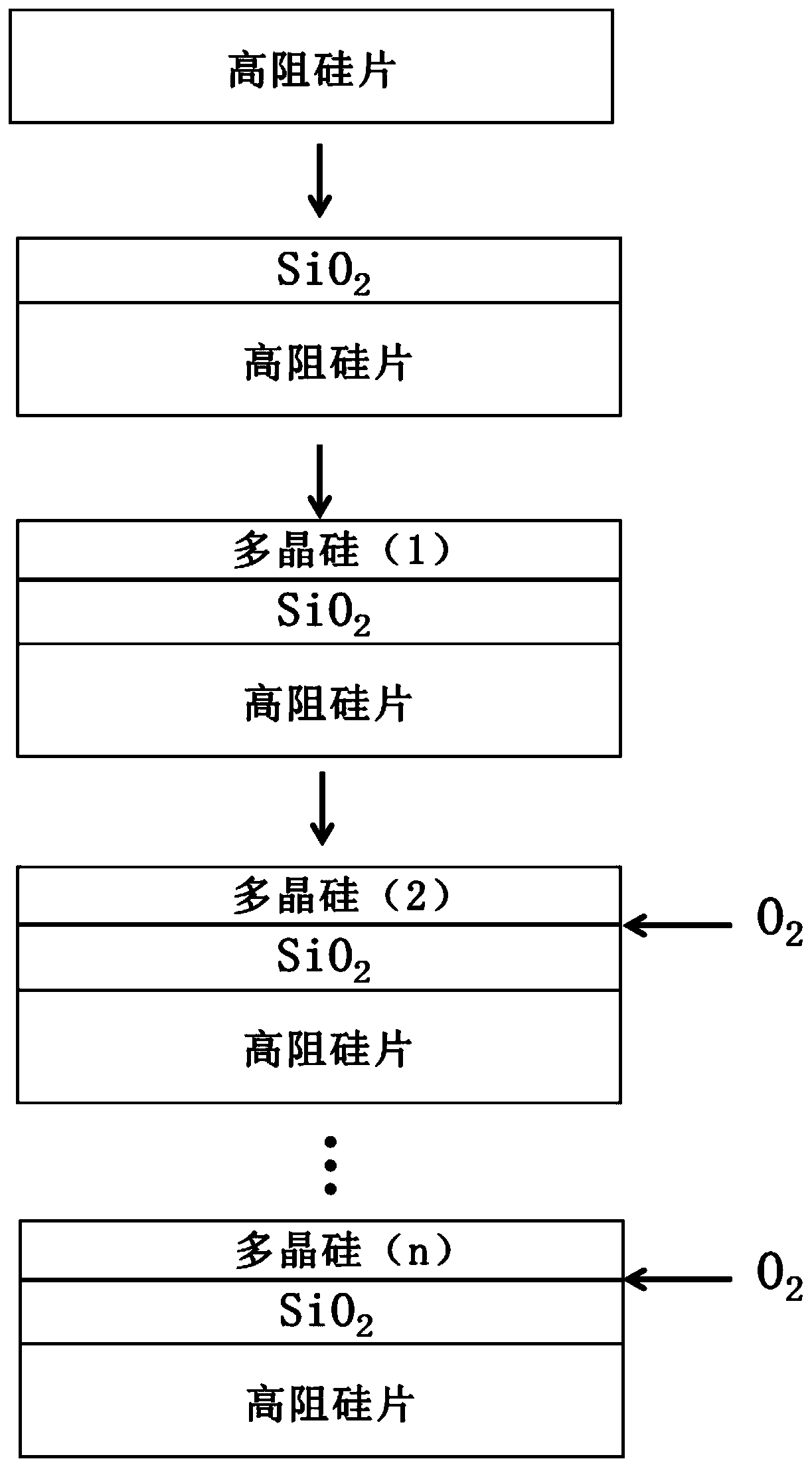
[0020] refer to Figure 1 to Figure 4 , in step S10, adopt DHF (hydrofluoric acid), SC1 and SC2 to clean the high-resistance silicon chip successively, the high-resistance silicon chip after cleaning is oxidized, obtain the silicon oxide layer (for example silicon dioxide SiO 2 ) high-resistance silicon wafer.

[0021] As an example, DHF, SC1 and SC2 are used to clean the high-resistance silicon wafer in sequence for 1-2 hours each, so as to remove the natural oxide layer and pollutants on the surface of the high-resistance silicon wafer. Specifically, DHF is used to remove the natural oxide layer; SC1 is a mixed solution of ammonia, hydrogen peroxide and ultrapure water for removing surface particles; SC2 is a mixed solution of hydrochloric acid, hydrogen peroxide and ultrapure water for cleaning metal contamination.

[0022] Preferably, the cleaned high-resistance silicon wafer is placed in an oxidation furnace with an oxidation temperature of 1100° C., and a silicon oxide ...

Embodiment 2

[0056] This embodiment provides a method for preparing an SOI wafer, including:

[0057] Use DHF, SC1 and SC2 to clean the high-resistance silicon wafer in sequence, and oxidize the cleaned high-resistance silicon wafer at a temperature of 1150° C. to obtain a high-resistance silicon wafer with a silicon oxide layer. The thickness of the silicon oxide layer is

[0058] By means of low-pressure chemical vapor deposition, under the conditions of growth pressure 3.5 Torr and reaction temperature 610°C, two polysilicon deposition steps are carried out until the thickness of the oxygen-doped polysilicon layer reaches 1.2 μm, and high-resistance silicon with an oxygen-doped polysilicon layer is obtained. sheet; wherein, the polysilicon deposition step is: deposit polysilicon on the surface of the silicon oxide layer, and then pass through 0.8% oxygen / argon for 3 minutes;

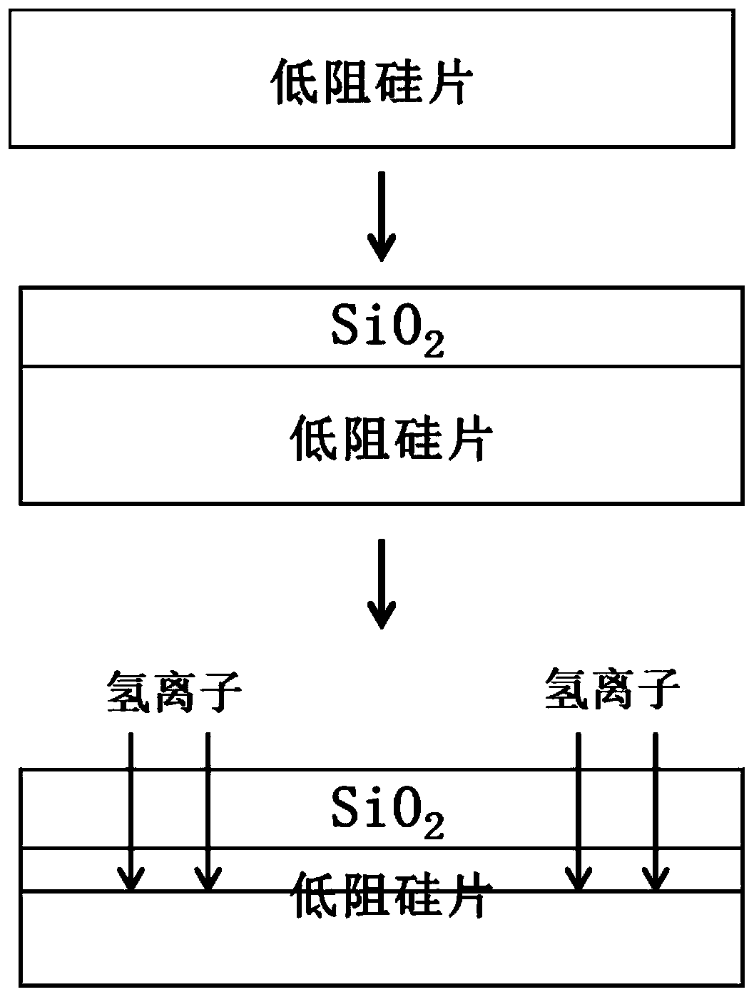
[0059] Use DHF, SC1 and SC2 to clean the low-resistance silicon wafer in sequence, and oxidize the cleaned lo...

Embodiment 3

[0067] This embodiment provides a method for preparing an SOI wafer, including:

[0068] Use DHF, SC1 and SC2 to clean the high-resistance silicon wafer in sequence, and oxidize the cleaned high-resistance silicon wafer at a temperature of 1100° C. to obtain a high-resistance silicon wafer with a silicon oxide layer. The thickness of the silicon oxide layer is

[0069] By means of low-pressure chemical vapor deposition, under the conditions of growth pressure 0.5 Torr and reaction temperature 650°C, four polysilicon deposition steps are carried out until the thickness of the oxygen-doped polysilicon layer reaches 1.8 μm, and high-resistance silicon with an oxygen-doped polysilicon layer is obtained. sheet; wherein, the polysilicon deposition step is: depositing polysilicon on the surface of the silicon oxide layer, and then feeding 0.6% oxygen / argon gas for 4 minutes;

[0070] Use DHF, SC1 and SC2 to clean the low-resistance silicon wafer in sequence, and oxidize the cleaned...


PUM

PropertyMeasurementUnit
Thicknessaaaaaaaaaa
Film thicknessaaaaaaaaaa

Abstract

The invention provides a preparation method o a SOI wafer. The preparation method comprises the following steps: oxidizing the cleaned high-resistance silicon wafer and obtaining the high-resistance silicon wafer with an oxygen-doped polysilicon layer by low-pressure chemical vapor deposition; oxidizing the cleaned low-resistance silicon wafer and performing hydrogen ion injection of the low-resistance silicon wafer with the silicon oxide layer; performing bonding and annealing treatment on the high-resistance silicon wafer with the oxygen-doped polysilicon layer and the injected low-resistance silicon wafer so as to obtain a bonding wafer; splitting the bonding wafer to obtain the SOI with the oxygen-doped polysilicon layer; cleaning the SOI and performing annealing treatment so as to obtain a processed SOI wafer; and performing cleaning and CMP process so as to obtain the SOI wafer with the oxygen-doped polysilicon layer. The preparation method of the SOI wafer can suppress the surface parasitic conductance of the silicon substrate, limit the capacitance change and reduce the power of generated harmonics, thus minimizing the loss of the resistivity of the high-resistance SOI substrate.

Description

technical field [0001] The invention relates to the technical field of microelectronics, in particular to a method for preparing an SOI wafer. Background technique [0002] Currently, the materials used for radio frequency (RF) front-end modules include: (1) SOQ (silicon on quartz, silicon on quartz), SOS (silicon on sapphire, silicon on sapphire): SOQ produces lower leakage current, It has low parasitic capacitance, which can improve the circuit performance at high frequency; SOS has excellent electrical insulation, which can effectively prevent the radiation caused by stray current from spreading to nearby components. Substrates such as SOQ and SOS can achieve excellent RF performance, but such structures are rare and expensive. (2) High-resistance substrate silicon: The resistivity is above 500ohm.cm. This substrate is worse than the first one, but the cost is lower. (3) High-resistance SOI (Silicon-On-Insulator, silicon on insulating substrate) substrate: This type of ...

Claims


Application Information

Patent Timeline
IPC IPC(8): H01L21/02H01L21/762
CPCH01L21/02532H01L21/0257H01L21/02595H01L21/0262H01L21/76202H01L21/76251
Inventor 高文琳
Owner SHENYANG SILICON TECH
Why Eureka
Try Eureka