Method for preparing thin film

A technology of thin film and silicon oxide layer, applied in the field of preparation of SOI wafers, can solve the problems of difficult to produce materials with good thermal stability, low substrate surface resistivity, difficult to control, etc. Effect of defect density, low manufacturing cost

Inactive Publication Date: 2018-05-11
SHENYANG SILICON TECH
View PDF7 Cites 3 Cited by
  • Summary
  • Abstract
  • Description
  • Claims
  • Application Information

AI Technical Summary

Problems solved by technology

[0005] 3. High-resistance SOI substrate: This type of substrate has structural advantages, but its performance is worse than that of the first type
However, diffusion of oxygen atoms, heat treatment process lead to low surface resistivity of the formed substrate
These two reasons are currently out of control
[0007] 4. On the basis of the third type, the high-resistance SOI substrate type substrate is improved by adding a defect layer: In order to achieve this goal, many technologies have been tried, but there are some shortcomings: sensitive to SOI manufacturing and subsequent IC device manufacturing Heat generated during the middle process, it is not easy to produce materials with good thermal stability

Method used


Image

  • Method for preparing thin film

Examples


Embodiment 1

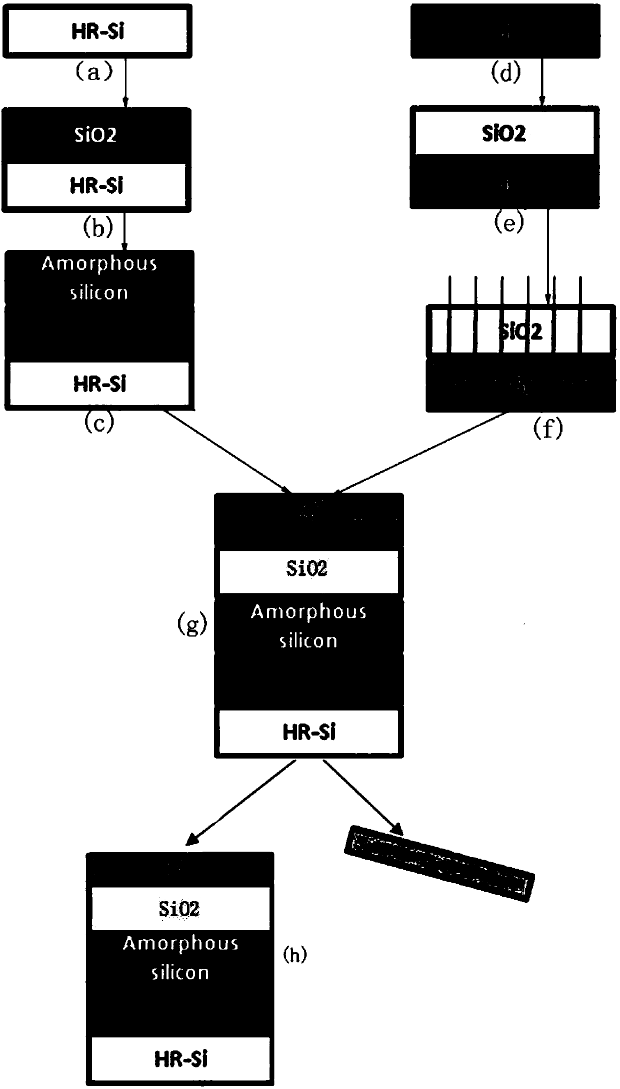
[0031] This embodiment provides a method for preparing a thin film, the thin film refers to an SOI sheet with an amorphous silicon layer, and its preparation includes the following steps:

[0032] 1. Provide high-resistance silicon wafers (silicon wafer resistivity greater than 1000ohm.cm), and use DHF, SC1 and SC2 to clean the surface in order to remove the natural oxide layer and pollutants on the silicon wafer surface; use testing equipment to test the silicon wafer surface Particle situation, silicon wafers that meet the requirements, proceed to the next step ( figure 1 (a)).

[0033] 2. Reference figure 1 (b), prepare a silicon oxide layer on the surface of the high-resistance silicon wafer, and the thickness of the grown oxide layer is about 200A; the preparation process is: place the high-resistance silicon wafer in an oxidation furnace, and the oxidation temperature is about 1100 ° C; and then sequentially Clean with SC1 and SC2 to remove surface pollutants. Use the...


PUM

PropertyMeasurementUnit
thicknessaaaaaaaaaa

Abstract

The invention discloses a method for preparing a thin film, and belongs to the technical field of preparation of SOI wafers. According to the invention, a layer of dielectric material (silicon oxide)grows on a provided high-resistivity silicon wafer, then a layer of amorphous silicon grows on the dielectric material layer, a layer of silicon oxide is transferred to the amorphous silicon to enablethe oxidation layer to have monocrystalline silicon, and an SOI wafer with an amorphous silicon layer is prepared. The process is completed in specific process conditions. The prepared thin film, namely, the SOI wafer with the amorphous silicon layer, is mainly applied to radio frequency equipment.

Description

technical field [0001] The invention relates to the technical field of preparation of SOI sheets, in particular to a method for preparing a thin film, and the prepared thin film is mainly used in radio frequency equipment. Background technique [0002] The materials currently used for RF front-end modules are as follows: [0003] 1. SOQ (silicon on silicon on quartz), SOS (silicon on sapphire sapphire): SOQ is the same as traditional SOI, it produces lower leakage current, due to its lower parasitic capacitance, high frequency Circuit performance has been improved. The advantage of SOS is its excellent electrical insulation, which can effectively prevent the radiation caused by stray currents from spreading to nearby components. Substrates such as SOQ and SOS can achieve excellent RF performance, but there are very few such structures, so they are very expensive. [0004] 2. High-resistance substrate silicon: its resistivity is above 500ohm.cm. This kind of substrate is w...

Claims


Application Information

Patent Timeline
Patent Type & Authority Applications(China)
IPC IPC(8): H01L27/12H01L21/324H01L21/02
CPCH01L21/02H01L21/02041H01L21/02107H01L21/02532H01L21/324H01L27/1203H01L21/76254H01L21/7624H01L21/0262H01L21/02065H01L21/02592H01L21/3003H01L21/30625
Inventor 孙伟
Owner SHENYANG SILICON TECH
Why Eureka
Try Eureka