Crystal growth furnace for preparing single crystal by PVT method and application thereof

A technology of crystal growth furnace and single crystal, applied in the field of semiconductor material preparation, can solve the problems of high cost, high cost, cumbersome preparation process, etc., and achieve the effects of less defect density, high sheet yield and high efficiency

Active Publication Date: 2020-04-24
SICC CO LTD
View PDF7 Cites 6 Cited by
  • Summary
  • Abstract
  • Description
  • Claims
  • Application Information

AI Technical Summary

Problems solved by technology

These defects will continue to be inherited into the newly grown single crystal during the single crystal growth process and continue to form through defects. Therefore, it is difficult to control the defect density in the single crystal and the substrate, and the cost is high, and it is difficult to improve the quality of the substrate.
[0004] Nature reported a silicon carbide single crystal preparation method that avoids defects such as micropipes and dislocations through crystal cross-sectional growth. However, the preparation process of this method is cumbersome. Although the defect density can be reduced, the cost is high and it is not suitable for industrial production.

Method used


Image

  • Crystal growth furnace for preparing single crystal by PVT method and application thereof
  • Crystal growth furnace for preparing single crystal by PVT method and application thereof
  • Crystal growth furnace for preparing single crystal by PVT method and application thereof

Examples


Embodiment 1

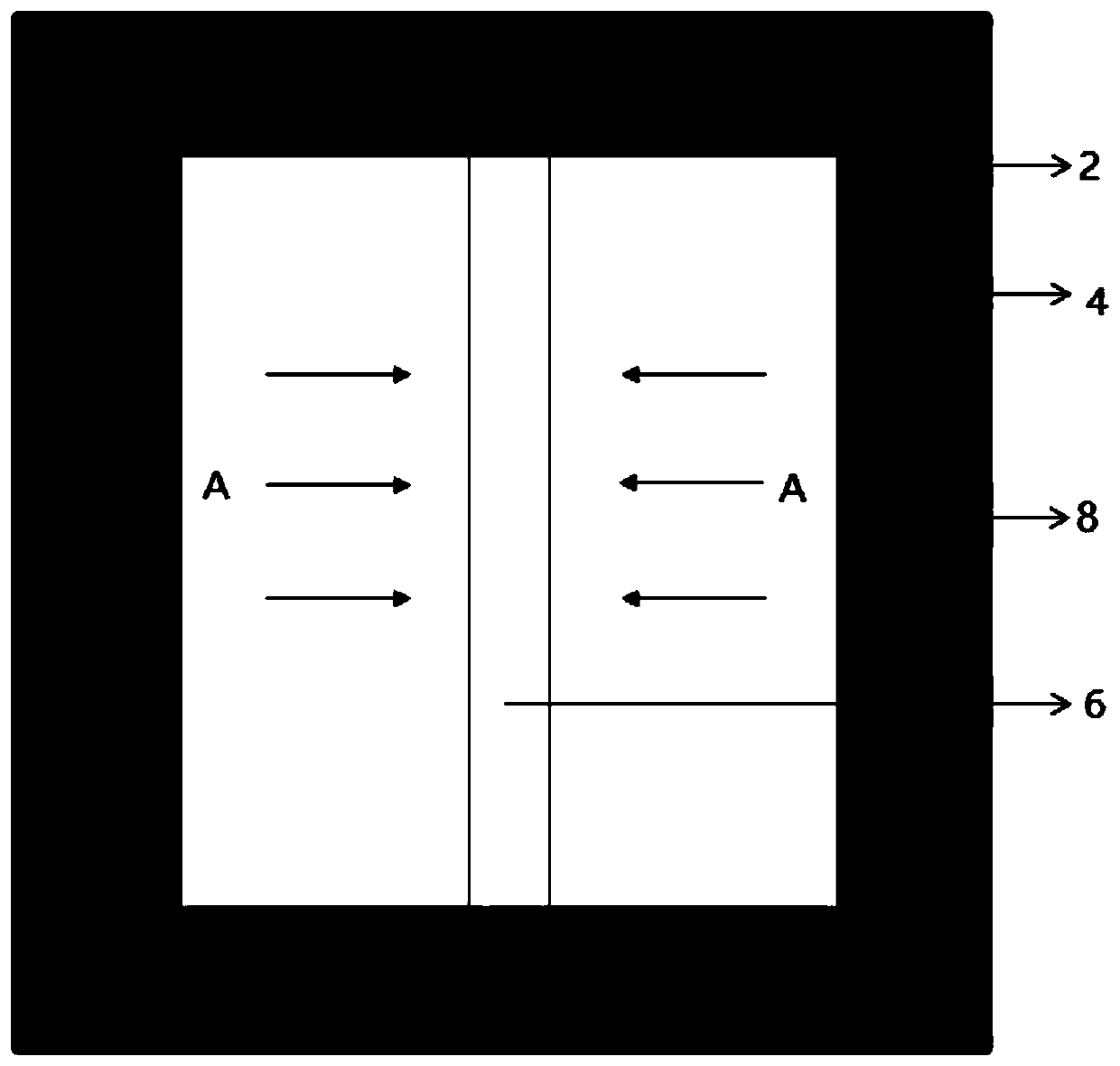
[0063] As a method for preparing a silicon carbide single crystal from any of the above-mentioned crystal growth furnaces, the method comprises the following steps:

[0064] 1) Provide crucible and silicon carbide seed column;

[0065] 2) Put the silicon carbide powder into the raw material cavity formed by the interlayer on the side wall of the crucible, install the silicon carbide seed crystal column in the crucible, and put it into the crystal growth furnace after assembly;

[0066] 3) Increase the temperature of the crystal growth furnace to 2000-2300°C, so that the sublimation gas after the sublimation of the raw materials passes through the inner wall of the interlayer and is transported to the surface of the seed crystal column in the gas phase in the radial direction, and the temperature difference between the inner surface of the inner wall and the surface of the seed crystal T is 50-300°C, and crystal growth is carried out to obtain a silicon carbide single crystal; ...

Embodiment 2

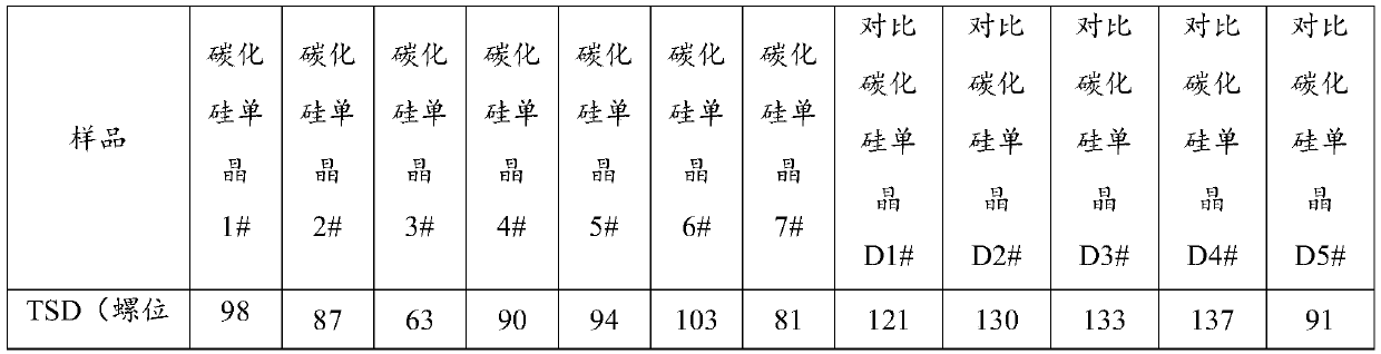
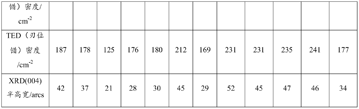
[0069] Taking the preparation of the seed crystal column with a length of 150mm as an example to illustrate the preparation method, according to the method of Example 1, silicon carbide single crystals 1#-7#, and comparative silicon carbide single crystals D1#-D5#, are different from the method of the embodiment The point is in Table 1.

[0070] Table 1

[0071] sample Temperature difference T / ℃ D1 / mm D2 / mm D3 / mm Silicon carbide single crystal 1# 50 180 170 15 Silicon carbide single crystal 2# 150 180 170 15 Silicon carbide single crystal 3# 300 180 170 15 Silicon carbide single crystal 4# 150 160 170 15 Silicon carbide single crystal 5# 150 180 190 15 Silicon carbide single crystal 6# 150 180 170 7 Silicon carbide single crystal 7# 150 180 220 15 Comparative SiC single crystal D1# 150 320 170 15 Compared with silicon carbide single crystal D2# 150 180 280 15 Compared with si...


PUM

PropertyMeasurementUnit
widthaaaaaaaaaa
lengthaaaaaaaaaa
widthaaaaaaaaaa

Abstract

The invention discloses a crystal growth furnace for preparing single crystals through a PVT method and an application of the crystal growth furnace, which belong to the field of semiconductor material preparation. The crystal growth furnace for preparing the single crystals by the PVT method comprises a crucible, a heat preservation structure, a furnace body and a heating coil which are arrangedfrom inside to outside, and further comprises a seed crystal column arranged in the crucible. The side wall of the crucible comprises an interlayer, the interlayer comprises an inner side wall and anouter side wall, the porosity of the inner side wall is higher than that of the outer side wall, and the interlayer forms a raw material cavity; the extension directions of the seed crystal column andthe central axis of the crucible are approximately the same, and a crystal growth cavity is formed between the seed crystal column and the inner surface of the inner side wall; the heating coil induces and heats the side wall of the crucible, so that the raw materials in the raw material cavity penetrate through the inner side wall after sublimation, and are conveyed to the surface of the seed crystal column in the crystal growth cavity along the radial gas phase for crystal growth. The crystal growth furnace can be used for efficiently and quickly preparing the silicon carbide single crystalwith extremely low defect density and the substrate of the silicon carbide single crystal, so that a technical foundation is laid for large-scale commercialization of high-quality and low-cost silicon carbide substrates.

Description

technical field [0001] The application relates to a crystal growth furnace for preparing single crystal by PVT method and its application, belonging to the field of semiconductor material preparation. Background technique [0002] The existing silicon carbide preparation technology is mainly based on the physical vapor transport (PVT) method. The PVT method is formed by sublimation and decomposition of the silicon carbide raw material placed at the bottom and transported to the seed crystal along the axial temperature gradient for crystallization. In the prior art, the flaky seed crystal used in the PVT method is placed on the top of the crucible, and the silicon carbide single crystal grows vertically downward along a certain radial direction of the single crystal. [0003] Since the silicon carbide single crystal grows downward due to the limitation of the distance from the single crystal growth surface and the raw material surface, the crystal growth thickness is usually...

Claims


Application Information

Patent Timeline
Patent Type & Authority Applications(China)
IPC IPC(8): C30B23/00C30B29/36
CPCC30B23/00C30B29/36
Inventor 高超宁秀秀李霞刘家朋宗艳民
Owner SICC CO LTD
Why Eureka
Try Eureka