Analog to digital converter device and method of calibrating clock skew

a digital converter and analog to digital converter technology, applied in the field of timeinterleaved analog to digital converter and a method of calibrating clock skew, can solve the problems of affecting the resolution and/or linearity of the adc, increasing the power consumption and/or longer the correction cycle of the adc, etc., to achieve the effect of reducing the overall power consumption

Active Publication Date: 2020-09-22
GLOBAL UNICHIP CORPORATION +1
View PDF27 Cites 4 Cited by
  • Summary
  • Abstract
  • Description
  • Claims
  • Application Information

AI Technical Summary

Benefits of technology

[0004]Some aspects of the present disclosure are to provide an analog to digital converter device that includes a plurality of analog to digital converter circuitries, a calibration circuitry, and a skew adjustment circuitry. The plurality of analog to digital converter circuitries are configured to convert an input signal according to a plurality of interleaved clock signals, in order to generate a plurality of first quantization outputs. The calibration circuitry is configured to perform at least one calibration operation according to the plurality of first quantization outputs, in order to generate a plurality of second quantization outputs. The skew adjustment circuitry is configured to determine a plurality of maximum value signals, to which the plurality of second quantization outputs respectively correspond during a predetermined interval, and to average the plurality of maximum value signals to generate a reference signal, and to compare the reference signal with each of the plurality of maximum value signals to generate a plurality of adjustment signals, in order to reduce a clock skew of the plurality of analog to digital converter circuitries.
[0006]As described above, the ADC device and the method in the embodiments of the present disclosure may perform simple operations to obtain the information of timing skew without employing additional ADC circuits. As a result, the overall power consumption and the calibration cycle can be reduced.

Problems solved by technology

In practical applications, the resolution and / or the linearity of the ADC may be affected by gain error(s), voltage error(s), and / or timing error(s).
In regard to the timing error, in current approaches, complex circuits (e.g., additional reference ADC circuit(s) or auxiliary ADC circuit(s)) are utilized or an off-chip calibration is performed to calibrate the timing error, resulting in a higher power consumption and / or longer correction cycles of the ADC.

Method used


Image

  • Analog to digital converter device and method of calibrating clock skew
  • Analog to digital converter device and method of calibrating clock skew
  • Analog to digital converter device and method of calibrating clock skew

Examples


Embodiment Construction

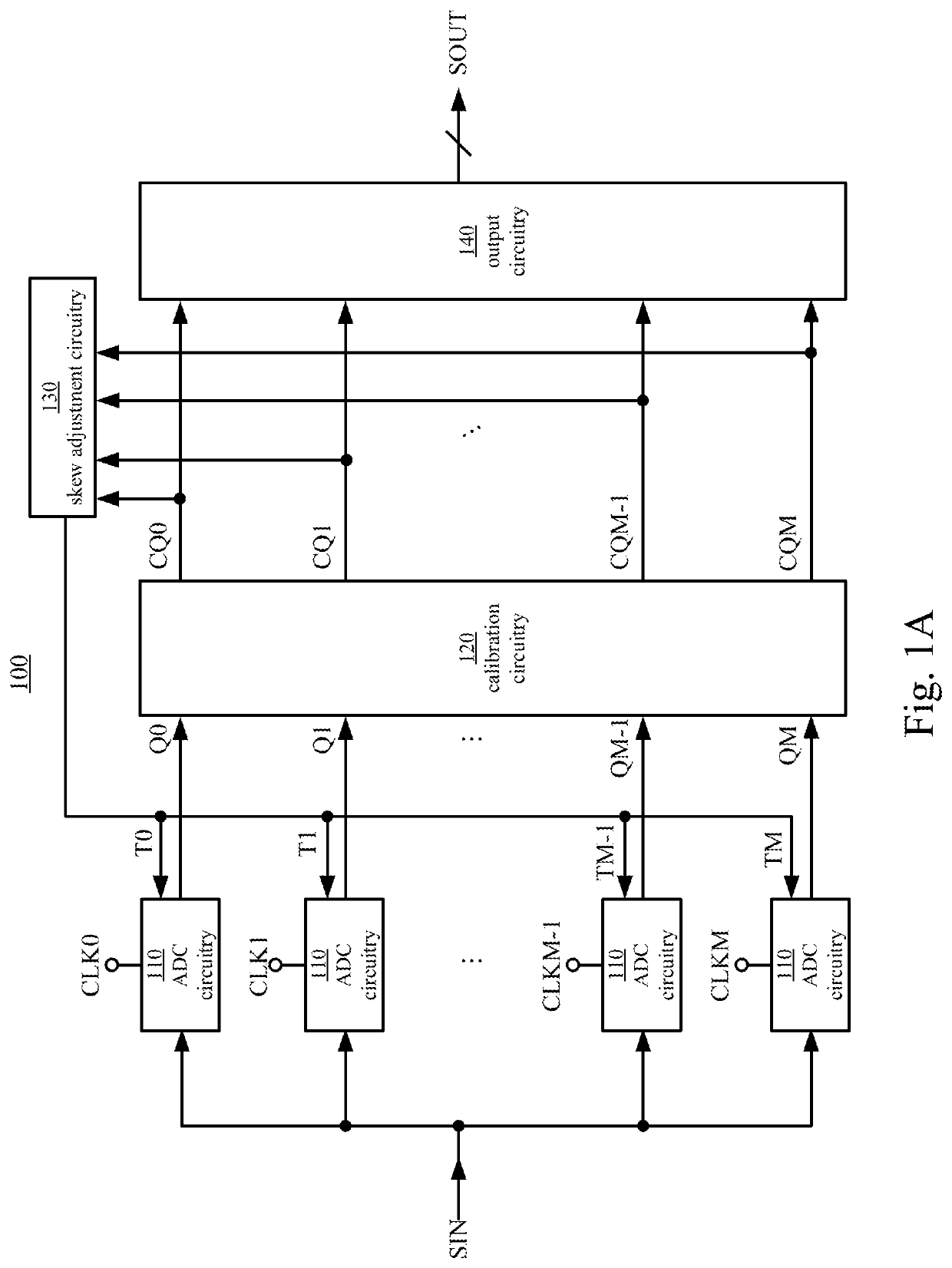
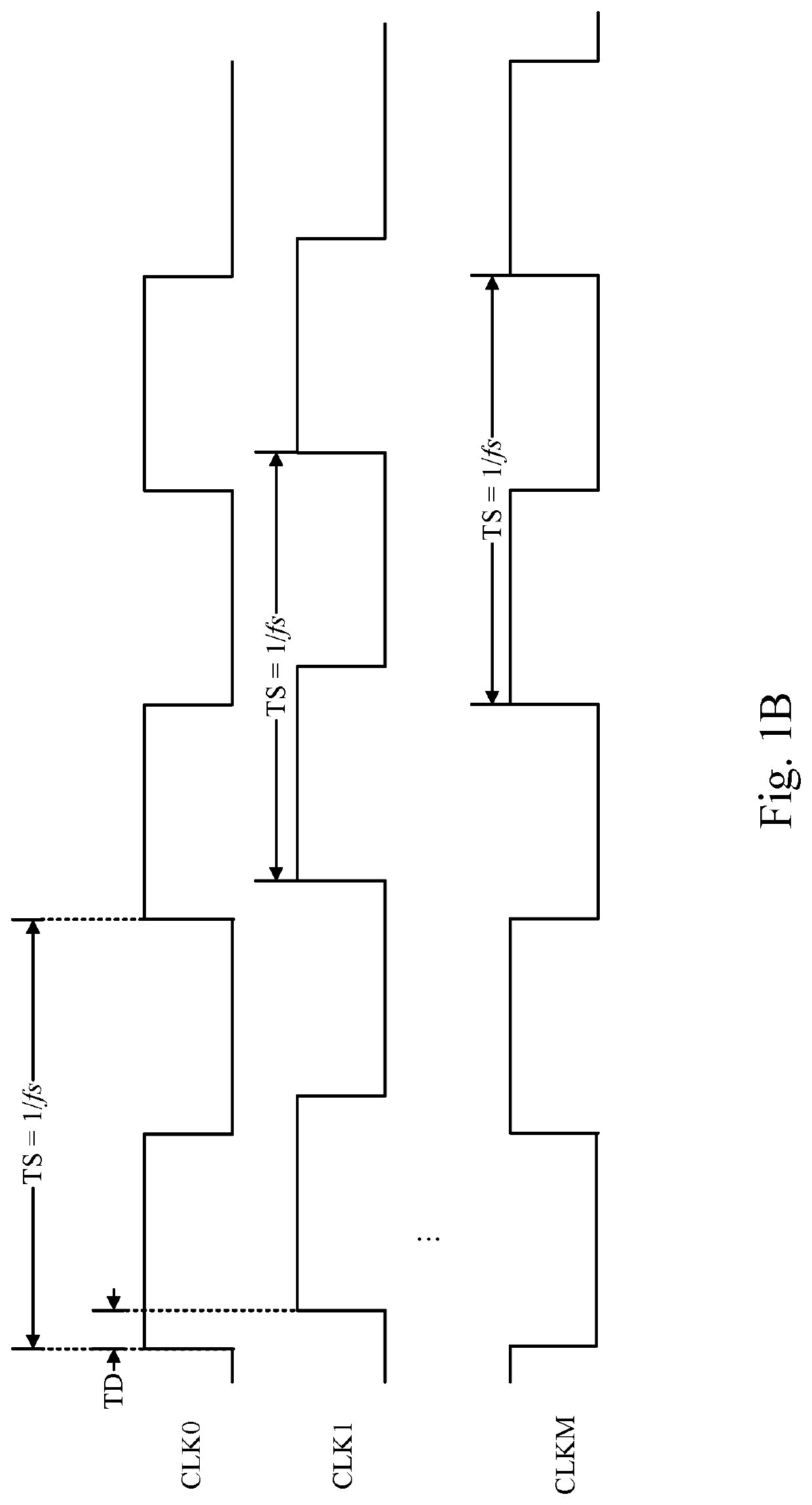
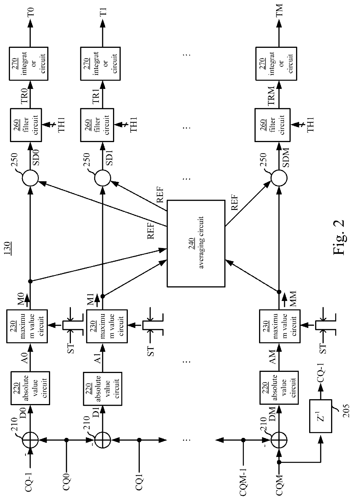
[0012]The following embodiments are disclosed with accompanying diagrams for detailed description. For illustration clarity, many details of practice are explained in the following descriptions. However, it should be understood that these details of practice do not intend to limit the present disclosure. That is, these details of practice are not necessary in parts of embodiments of the present embodiments. Furthermore, for simplifying the drawings, some of the conventional structures and elements are shown with schematic illustrations.

[0013]In this document, the term “coupled” may also be termed as “electrically coupled,” and the term “connected” may be termed as “electrically connected.”“Coupled” and “connected” may mean “directly coupled” and “directly connected” respectively, or “indirectly coupled” and “indirectly connected” respectively. “Coupled” and “connected” may also be used to indicate that two or more elements cooperate or interact with each other.

[0014]In this document...


PUM


Abstract

An analog to digital converter (ADC) device includes ADC circuitries, a calibration circuitry, and a skew adjustment circuitry. The ADC circuitries are configured to convert an input signal according to interleaved clock signals, in order to generate first quantization outputs. The calibration circuitry is configured to perform at least one calibration operation according to the first quantization outputs, in order to generate second quantization outputs. The skew adjustment circuitry is configured to determine maximum value signals, to which the second quantization outputs respectively correspond during a predetermined interval, and to average the maximum value signals to generate a reference signal, and to compare the reference signal with each of the maximum value signals to generate adjustment signals, in order to reduce a clock skew of the ADC circuitries.

Description

RELATED APPLICATIONS[0001]This application claims priority to Taiwan Application Serial Number 108102604, filed Jan. 23, 2019, which is herein incorporated by reference in its entirety.BACKGROUNDTechnical Field[0002]The present disclosure relates to an analog to digital converter device. More particularly, the present disclosure relates to a time-interleaved analog to digital converter and a method of calibrating clock skew(s) thereof.Description of Related Art[0003]Analog to digital converters (ADC) have been widely utilized in various electronic devices, in order to convert an analog signal to a digital signal. In practical applications, the resolution and / or the linearity of the ADC may be affected by gain error(s), voltage error(s), and / or timing error(s). In regard to the timing error, in current approaches, complex circuits (e.g., additional reference ADC circuit(s) or auxiliary ADC circuit(s)) are utilized or an off-chip calibration is performed to calibrate the timing error,...

Claims


Application Information

Patent Timeline
Patent Type & Authority Patents(United States)
IPC IPC(8): H03M1/10H03M1/12H03M1/06
CPCH03M1/0617H03M1/1245H03M1/1033H03M1/0624H03M1/0836H03M1/1215
Inventor KANG, WEN-JUHCHEN, YU-CHULAM, MAN-PIO
Owner GLOBAL UNICHIP CORPORATION
Why Eureka
Try Eureka