Integrated circuit package element and load board thereof

a technology of integrated circuits and load boards, which is applied in the direction of semiconductor devices, semiconductor/solid-state device details, electrical apparatus, etc., can solve the problems of decrementing and achieve the reduction of power noise coupling between the first electric power distribution network and the second electric power distribution network, reducing the generation of signal jitter, and increasing the signal integrity of the semiconductor package element

Active Publication Date: 2020-09-29
GLOBAL UNICHIP CORPORATION +1
View PDF12 Cites 0 Cited by
  • Summary
  • Abstract
  • Description
  • Claims
  • Application Information

AI Technical Summary

Benefits of technology

[0007]With the structure described in the above embodiments, power noise coupling between the first electric power distribution network and the second electric power distribution network can be reduced, thereby reducing signal jitter generated at an output end of the chip element and increasing the signal integrity of the semiconductor package element.

Problems solved by technology

However, since the modern size trends for the semiconductor packaging elements have been developed towards high density, electric power distribution networks (PDNs) are closely arranged in the semiconductor package element one to another, so that power noise coupling which introduces signal jitter due to the crosstalk effect is often caused, thereby decreasing the signal integrity of the semiconductor package element.

Method used


Image

  • Integrated circuit package element and load board thereof
  • Integrated circuit package element and load board thereof
  • Integrated circuit package element and load board thereof

Examples


Embodiment Construction

[0018]Reference will now be made in detail to the present embodiments of the disclosure, examples of which are illustrated in the accompanying drawings. Wherever possible, the same reference numbers are used in the drawings and the description to refer to the same or like parts. According to the embodiments, it will be apparent to those skilled in the art that various modifications and variations can be made to the structure of the disclosure without departing from the scope or spirit of the disclosure.

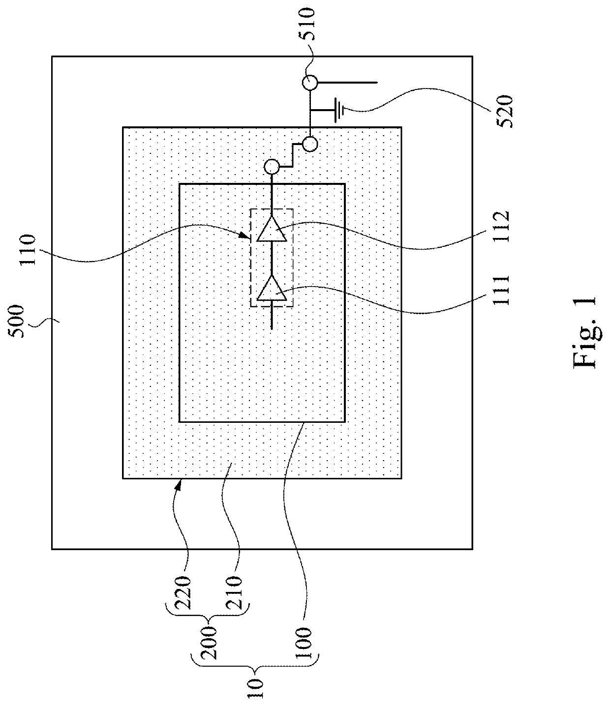
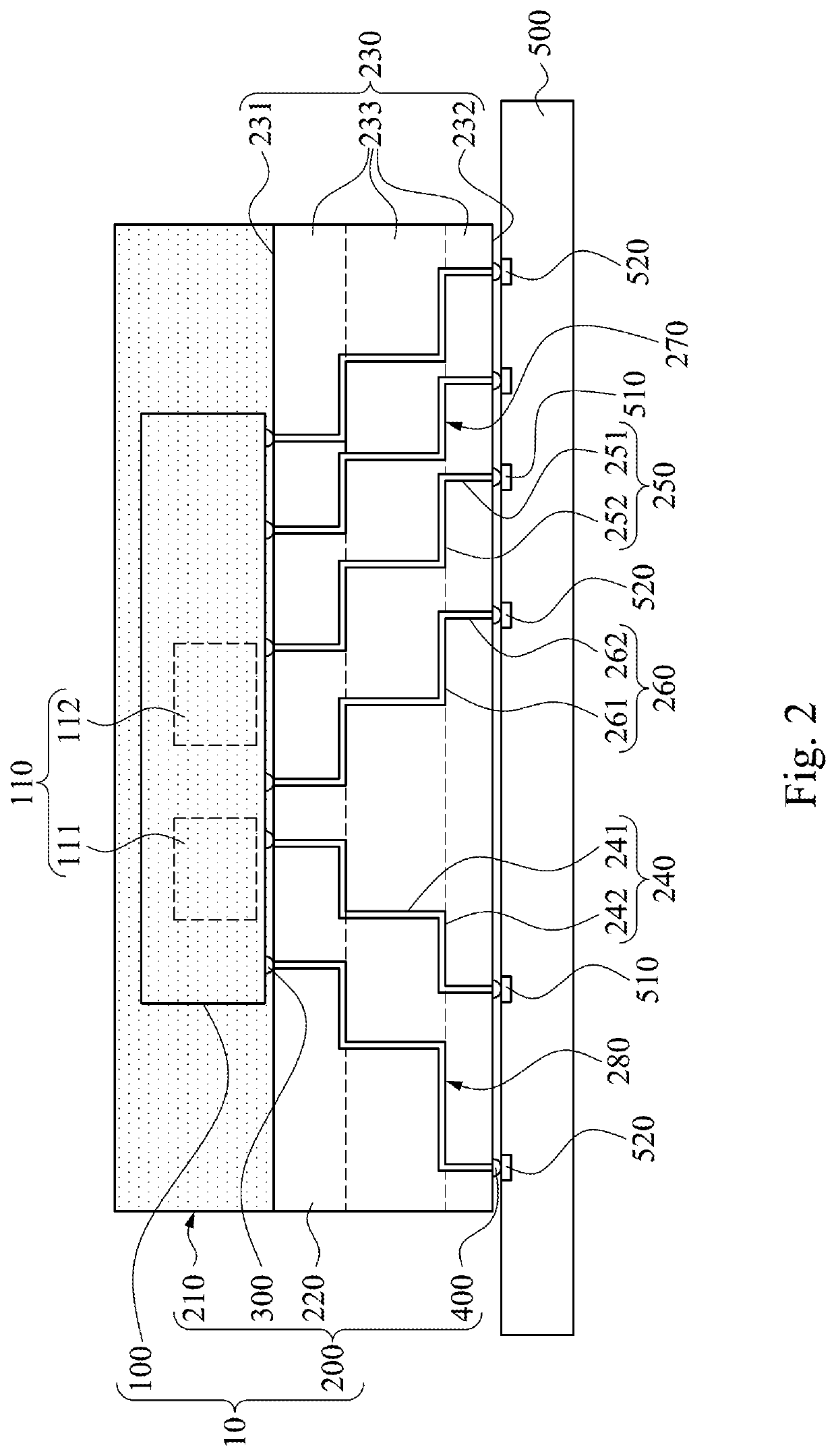
[0019]Reference is now made to FIG. 1 and FIG. 2 in which FIG. 1 is a schematic top view of an integrated circuit package element 10 being disposed on a circuit board 500 according to one embodiment of the disclosure, and FIG. 2 is a cross-sectional view of an integrated circuit package element 10 according to one embodiment of the disclosure. As shown in FIG. 1 and FIG. 2, the integrated circuit (IC) package element 10 is used to be soldered on a circuit board 500 (for example, a rig...


PUM


Abstract

An integrated circuit package element provided includes a chip element and a package module coupled to the chip element. The chip element includes two driving units that are electrically connected to each other. The package module includes a grounding area, two individual power distributed networks and a grounded shielding structure which is completely disposed between the individual power distributed networks, electrically connected to the chip element, and configured to block power noise coupling between the first electric power distribution network and the second electric power distribution network. The grounding area is electrically connected to the individual electric power distribution networks and the grounded shielding structure.

Description

RELATED APPLICATIONS[0001]This application claims priority to Taiwan Application Serial Number 107144599, filed Dec. 11, 2018, which is herein incorporated by reference.BACKGROUNDField of Disclosure[0002]The present disclosure relates to an integrated circuit package element. More particularly, the present disclosure relates to an integrated circuit package element having a shielding ground, and a load board of the integrated circuit package element.Description of Related Art[0003]Flip-chip technology has been widely implemented in the chip-packaging field since flip-chip technology has advantages such as reductions of chip package area and signal transmission path. Generally, a die that is finished is mounted on a load board, and the load board with the die will be packaged into a semiconductor package element through an integrated circuit (IC) encapsulation method. After the semiconductor package element is installed on a circuit board, the die can exchange signals with the extern...

Claims


Application Information

Patent Timeline
Patent Type & Authority Patents(United States)
IPC IPC(8): H01L23/498H01L23/552H01L23/00H01L23/31
CPCH01L23/49816H01L23/552H01L23/49827H01L23/49838H01L24/16H01L2224/16235H01L23/3128H01L23/3121H01L23/49822H01L2224/16227H01L2924/15174H01L2924/15192H01L2924/15311
Inventor YANG, SHENG-FANLIN, YUAN-HUNGSUN, YU-CHENGWAN, STEVE S. A.
Owner GLOBAL UNICHIP CORPORATION
Why Eureka
Try Eureka