Method and system for correction of optical proximity effect

a technology of optical proximity and correction method, applied in the field of semiconductor technology, can solve the problems of direct affecting the performance and yield of circuits, affecting determining the distortion and deviation of the mask pattern, so as to ensure the overall shape and size of the image, improve the effect of rounding performance at the corner, and improve the effect of rounding performan

Active Publication Date: 2020-10-27
CSMC TECH FAB2 CO LTD
View PDF9 Cites 2 Cited by
  • Summary
  • Abstract
  • Description
  • Claims
  • Application Information

AI Technical Summary

Benefits of technology

[0004]Accordingly, it is necessary to provide a method for correction of OPE that can improve the corner arc performance.
[0015]According to the foregoing method and system, when the adjacent side is relatively short, the target point is set between the vertex of the corner and the end point of the segment side so as to effectively improve the rounding performance at the corner and, in the meanwhile, ensure the overall shape and size of the image. When the adjacent side is relatively long, the border of the pattern obtained from the simulated photolithography is relatively steep, and rounding of the corner is acceptable. As such, the overall corner rounding performance is improved.

Problems solved by technology

As such, in the photolithographic process, due to the diffraction and interference of light, certain distortion and deviation exist between the mask pattern and the photo pattern obtained on the silicon wafer actually.
Such an error in the photolithography directly affect the performance and the yield of circuits.

Method used


Image

  • Method and system for correction of optical proximity effect
  • Method and system for correction of optical proximity effect
  • Method and system for correction of optical proximity effect

Examples


Embodiment Construction

[0021]The present disclosure will be described in the following with reference to the accompanying drawings and the embodiments in order to make the above objects, features and advantages of the present disclosure more apparent.

[0022]The specific embodiments will be described in detail in combination with the accompanying drawings.

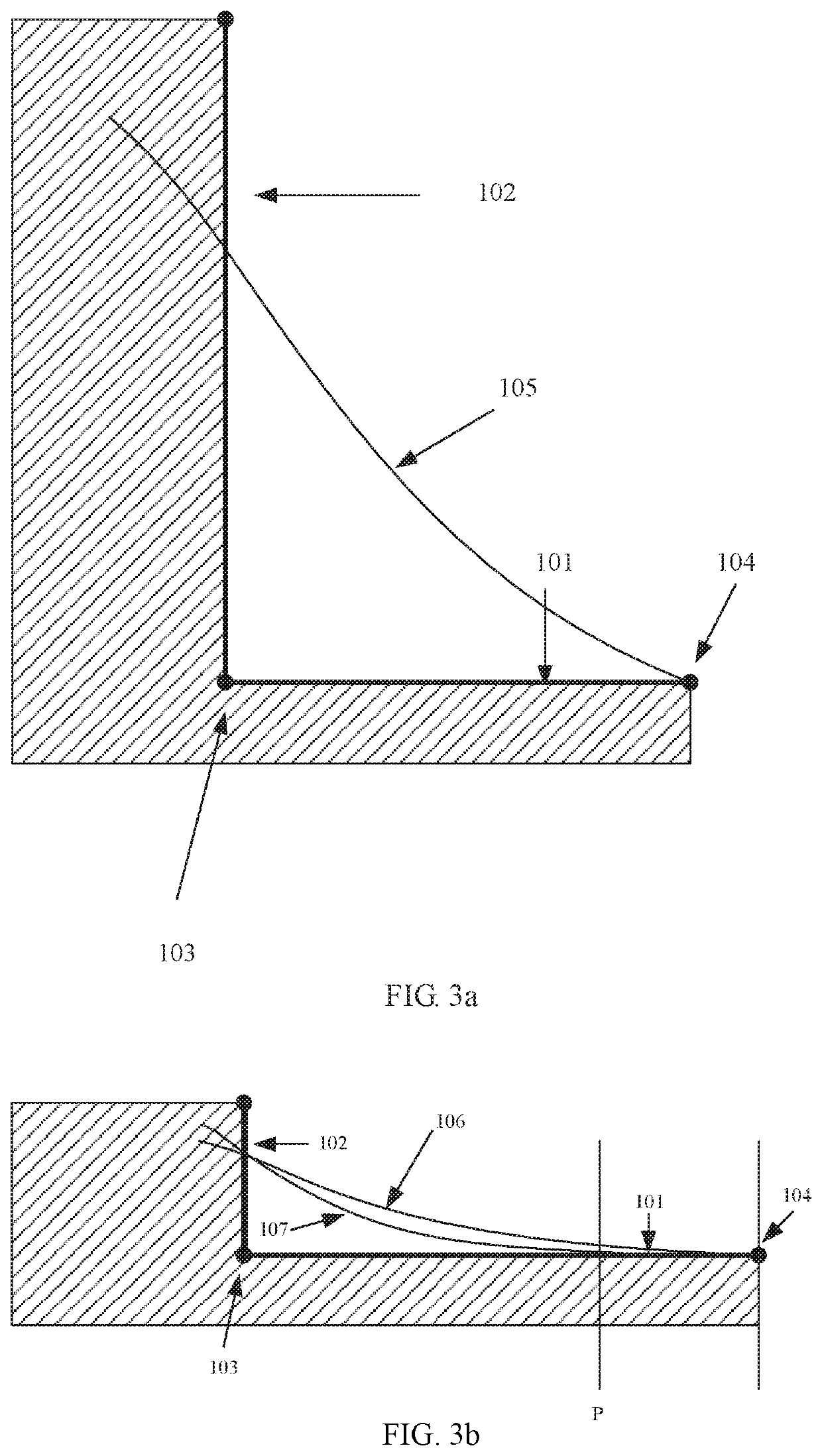
[0023]The method in the following embodiments is related to a method of how to place a target point in the OPE correction. There are a lot of steps included in the OPE correction method, and the placement of target point is one of the aspects. The embodiments below will not describe all the steps, only contents relevant to the placement of the target point are described.

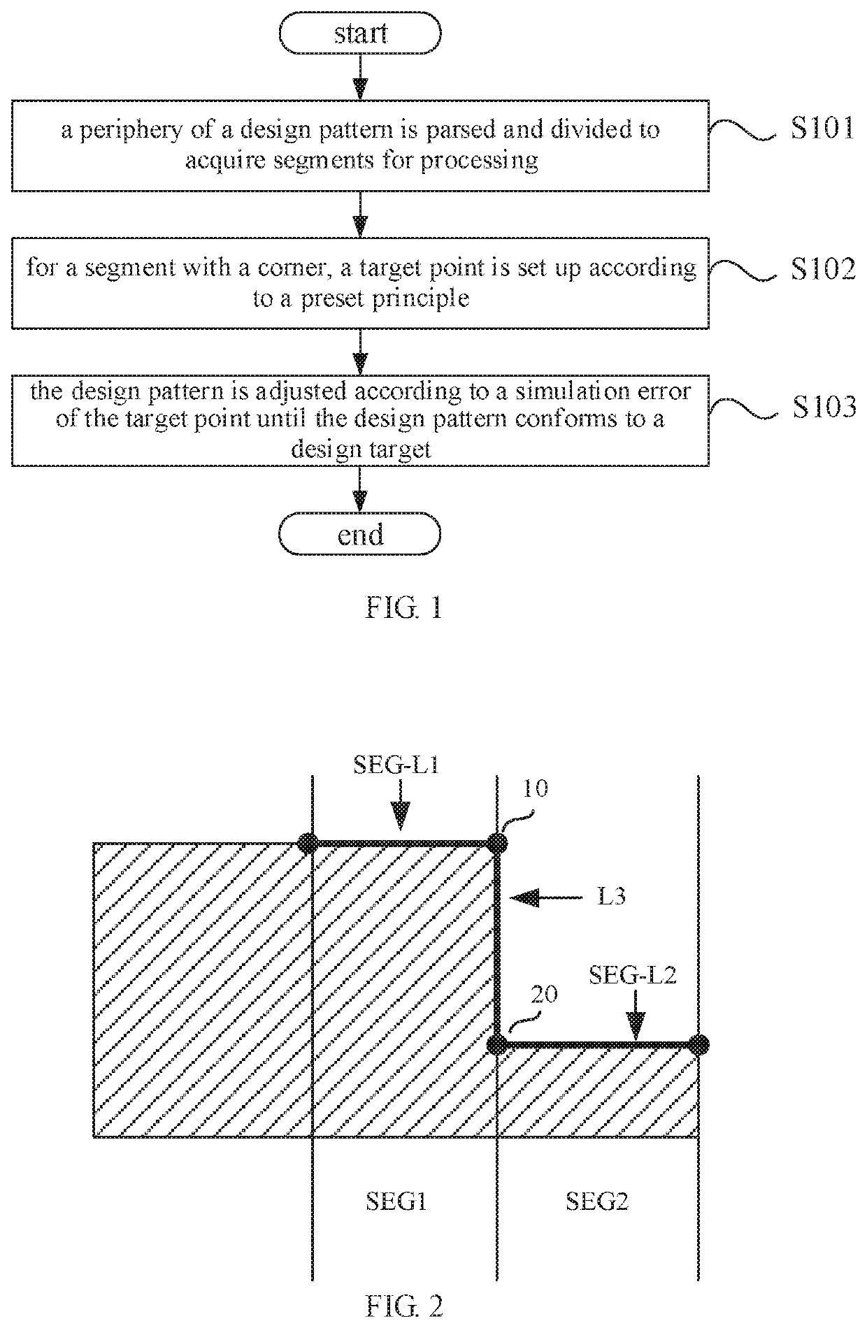
[0024]FIG. 1 is a flowchart of a method for correction of OPE according to an embodiment, the method includes the following steps of:

[0025]In step S101, an outer edge of a design pattern is parsed and divided to obtain segments to be processed. As the design pattern is usually complicated, ...


PUM

PropertyMeasurementUnit
optical proximity effectaaaaaaaaaa
lengthaaaaaaaaaa
acute angleaaaaaaaaaa

Abstract

A method for correction of an optical proximity effect, comprising: parsing and dividing the periphery of a design pattern to obtain segments to process; for a segment having a corner comprising a segment side (101) and an adjacent side (102) forming a corner relation with the segment side, setting a target point according to the following principle: when the length of the adjacent side (102) is greater than a preset length, the target point is set at the location of the outer end point (104) of the segment side; when the length of the adjacent side (102) is less than or equal to the preset length, the target point is set between the vertex (103) of the corner and the outer end point (104) of the segment side, and the less the length of the adjacent side (102), the further the target point from the location of the outer end point (104); and adjusting, according to a simulation difference of the target point, the design pattern until it conforms to a design target.

Description

FIELD OF THE INVENTION[0001]The present disclosure relates to a field of semiconductor technology, and particularly relates to a method and system for correction of optical proximity effect (OPE).BACKGROUND OF THE INVENTION[0002]With the development of semiconductor technology, the critical dimension of the key levels in the semiconductor process, such as the active region level, the gate-oxide level, or the metal wiring level, is increasingly smaller, which is approximating or even less than the wave length of the optical wave used in the photolithography technique. As such, in the photolithographic process, due to the diffraction and interference of light, certain distortion and deviation exist between the mask pattern and the photo pattern obtained on the silicon wafer actually.[0003]Such an error in the photolithography directly affect the performance and the yield of circuits. In order to eliminate such error as much as possible, an effective way is to adopt OPE correction. A s...

Claims


Application Information

Patent Timeline
Patent Type & Authority Patents(United States)
IPC IPC(8): G06F30/00G06F30/20G06F30/398G03F1/36
CPCG06F30/00G03F1/36G06F30/20G06F30/398
Inventor WAN, JINYIN
Owner CSMC TECH FAB2 CO LTD
Why Eureka
Try Eureka