Supercharge Your Innovation With Domain-Expert AI Agents!

Indium-gallium-nitride structures and devices

Active Publication Date: 2020-11-24
OPNOVIX CORP
View PDF12 Cites 2 Cited by
  • Summary
  • Abstract
  • Description
  • Claims
  • Application Information

AI Technical Summary

Benefits of technology

The present invention relates to semiconductor structures comprising III-nitride semiconductors that have a relaxed InGaN region with a periodicity in at least one direction. These structures also include a plurality of mask and non-mask regions. The invention also provides semiconductor devices, lighting systems, display systems, and other applications utilizing these semiconductor structures. The technical effects of the invention are improved semiconductor device performance and stability, as well as improved lighting and display systems.

Problems solved by technology

Unfortunately, the crystalline atomic lattice constant of InGaN is larger than that of GaN, resulting in severe strain, and increasingly poor material quality with increasing InN mole fraction or increasing thickness for InGaN grown on GaN (InGaN / GaN).
This limits the performance of optoelectronic devices based on InGaN / GaN including, for example, LEDs and LDs.
Attempts to grow high-quality, planar, relaxed InGaN for device applications have so far been unsuccessful in commercialization.
However, the relaxation mechanism is associated with the appearance of a high density of misfit dislocations, stacking faults, and threading dislocations, leading to poor material quality.
Similar approaches using commercially preferred metal organic chemical vapor deposition (MOCVD) for c-plane InGaN are compromised by the lack of a slip system for c-plane growth and attempts to use off-axis growth such as growth on non- and semi-polar growth planes result in material having a high defect density.
Hydride vapor phase epitaxy (HVPE) has been used to grow thick InGaN layers with the objective of reducing crystalline defects, but the approach is limited in terms of achievable InN mole fractions and is only applicable to N-polar surfaces and therefore is not ideal for low-cost manufacturing.
Growth of strained InGaN layers that can be lifted-off and bonded to compliant carriers to facilitate relaxation has been attempted, but the method results in limited lattice dilation and non-planar, trenched, surfaces.
The use of nano-column or nano-rod device structures, designed to avoid strain limits of conventional heteroepitaxy results in non-planar device geometries not suitable for manufacturing and that exhibit low optical quality.
However, similar approaches for Wurtzite semiconductors and / or ternary alloys such as InGaN have not been successful.
Furthermore, etching the substrate can serve to frustrate nucleation and growth of InGaN, which further reduces the possibility of interfering competitive growth modes.
For micro-LEDs, conventional dicing techniques are less suitable, so other means for singulating devices are often employed.

Method used


Image

  • Indium-gallium-nitride structures and devices
  • Indium-gallium-nitride structures and devices
  • Indium-gallium-nitride structures and devices

Examples


Embodiment Construction

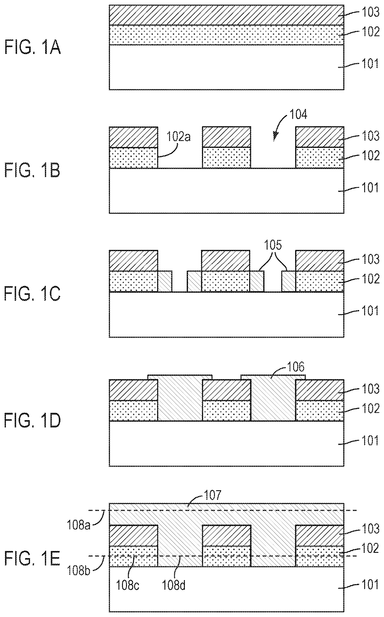
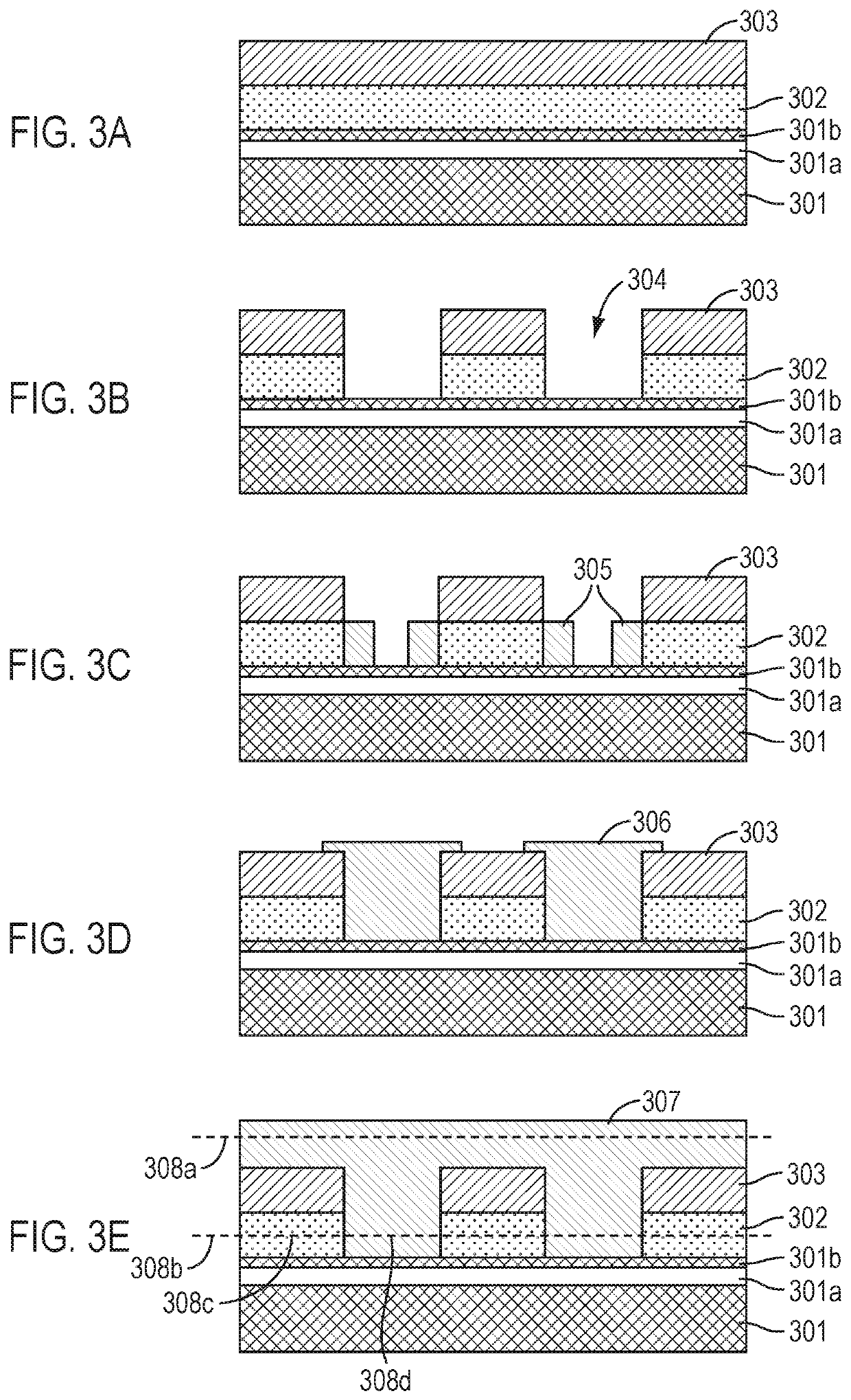
[0029]“Substantially uniform lattice constant” refers to a semiconductor layer characterized by a local lattice constant of the semiconductor layer that varies less than 1% with respect to an average lattice constant such as, for example, less than 0.5% with respect to an average lattice constant, or less than 0.1% with respect to an average lattice constant.

[0030]“Defect density” refers to the density, in plan view, of extended defects, such as dislocations, in a semiconductor layer. The defect density can be determined using, for example, etching (and counting etch pit density, EPD), cathodoluminescence to observe and count dark spots, atomic force microscopy (AFM) to observe and count small pits.

[0031]A lattice constant can be determined using X-ray diffraction (XRD) and reciprocal space map (RSM) analysis.

[0032]“III-V material” refers to a compound semiconductor material comprising at least one column-III element and at least one column-V element from the Periodic Table.

[0033]“G...


PUM


Abstract

InGaN layers characterized by an in-plane lattice constant within a range from 3.19 to 3.50 Å are disclosed. The InGaN layers are grown by coalescing InGaN grown on a plurality of GaN regions. The InGaN layers can be used to fabricate optical and electronic devices for use in light sources for illumination and display applications.

Description

FIELD[0001]The present disclosure relates to indium-gallium-nitride (InGaN) layers having a substantially relaxed region and to devices incorporating the InGaN layers. The substantially relaxed Wurtzite (0001) InGaN regions have an in-plane, or “a”, lattice constant greater than or equal to 3.19 Å. The substantially relaxed InGaN regions are grown on a plurality of III-nitride seed regions such as GaN or AlN seed regions. During growth, InGaN grown on the seed regions coalesces to provide substantially relaxed InGaN regions that can be used as a growth surface for other semiconductor materials. The InGaN layers can be used to fabricate optical and electronic devices for use as light sources in systems for illumination and display applications.BACKGROUND[0002]Compound semiconductor materials are typically deposited, or grown, atomically-lattice-matched to a growth substrate to avoid the generation of growth defects such as dislocations. In some cases, it is desirable that the lattice...

Claims


Application Information

Patent Timeline
IPC IPC(8): H01L33/00H01L29/04H01L21/00H01L33/32H01L29/205H01L21/02H01L29/02H01L33/24H01L29/20
CPCH01L21/02505H01L21/02502H01L29/2003H01L29/205H01L33/32H01L21/02647H01L21/02645H01L21/02458H01L21/0254H01L21/02488H01L29/045H01L21/0262H01L21/0265H01L33/16
Inventor KRAMES, MICHAEL R.
Owner OPNOVIX CORP
Features
  • R&D
  • Intellectual Property
  • Life Sciences
  • Materials
  • Tech Scout
  • Unparalleled Data Quality
  • Higher Quality Content
  • 60% Fewer Hallucinations
Learn More