Film and method for producing a film

a technology of film and film adhesive, applied in the field of film, can solve the problems of large time and personnel expenditure, inability to ensure the exact positioning of the touch sensor during application to the target substrate, and inability to ensure the production quality of as identical as possible, so as to achieve the effect of reducing time, personnel and logistics, and ensuring the production quality

Active Publication Date: 2021-01-05
LEONHARD KURZ STIFTUNG & CO KG
View PDF21 Cites 0 Cited by
  • Summary
  • Abstract
  • Description
  • Claims
  • Application Information

AI Technical Summary

Benefits of technology

[0007]It has been shown here that the film according to the invention improves the production process for electrical functional elements, such as for example touchscreens. Thus, the film according to the invention makes a direct application of the film to a target substrate possible without further intermediate steps and / or further intermediate products. This makes a faster production process possible and makes it possible to reduce costs in the production. Because the adhesion-promoting layer does not cover the at least one contacting region at least in areas, it is ensured that the electrical functional structure can be reliably and robustly contacted after application of the film to the target substrate. As the contacting region does not adhere to the target substrate in the regions without adhesion-promoting layer, the target substrate is easily accessible for a contacting. Waste can also be reduced compared with the use of an adhesive film with a non-self-supporting adhesive layer which is arranged between two so-called liners, as for example neither the error-prone and laborious adaptation of the previously separately present adhesive film to the target substrate nor the adaptation of the adhesive film to the touch sensor has to be carried out by hand. The production costs can be further reduced hereby. The film according to the invention also makes an industrial mass production possible. Thus, for example, it is possible to apply the film to a target substrate over the whole surface by means of hot laminators. During hot lamination individual, in particular loose, layers of a layer stack are acted on by means of pressure and heat in order to join the individual layers of the layer stack to each other non-detachably and thus to produce a composite body. Here, the pressure and / or the heat acts on the layer stack for example by means of flat tools. Alternatively or additionally, for example, rollers can also be provided as tools, which allow pressure and / or heat to act on the layer stack as a linear contact in a roller gap. The outlay in terms of time, personnel and logistics can be further reduced hereby and at the same time an identical production quality can be ensured. The invention thus makes it possible to produce electrical functional elements, for example a display with a touch sensor, cost-effectively and at the same time to enable a robust and reliable contacting of the electrical functional structure which provides, for example, the touchpad functionality.
[0222]It is further possible for the adhesion-promoting layer to consist of a material the visual appearance of which changes from cloudy to highly transparent and / or clear during and / or after step b). Thus, it is possible, during the application of the film to the target substrate, for the adhesion-promoting layer to be melted on because of added heat and / or for the adhesion-promoting layer to be smoothed out by means of pressure, with the result that the surface roughness of the adhesion-promoting layer present when the film is not applied is leveled out during and / or after the application. The visual appearance of the adhesion-promoting layer hereby changes from cloudy to highly transparent and / or clear.

Problems solved by technology

As these production processes are usually carried out by hand, a production quality that is as identical as possible is not always guaranteed.
Thus, for example, the exact positioning of the touch sensor during application to the target substrate is error-prone.
The individual work steps, in particular the detachment of the liners as well as a bubble-free application of the adhesive layer to the touch sensor or of the touch sensor to the target substrate, also require a large outlay in terms of time and personnel.

Method used


Image

  • Film and method for producing a film
  • Film and method for producing a film
  • Film and method for producing a film

Examples


Embodiment Construction

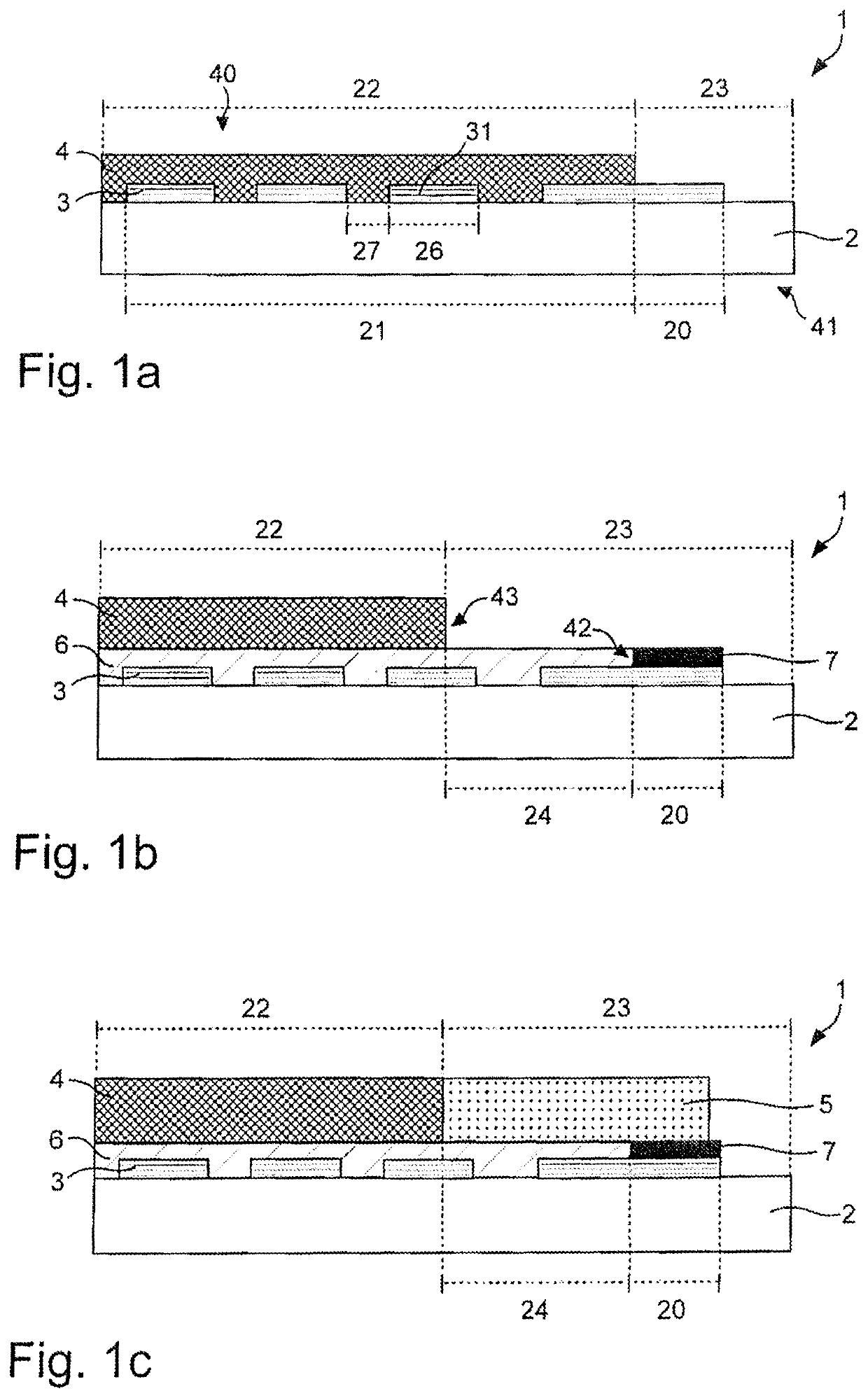
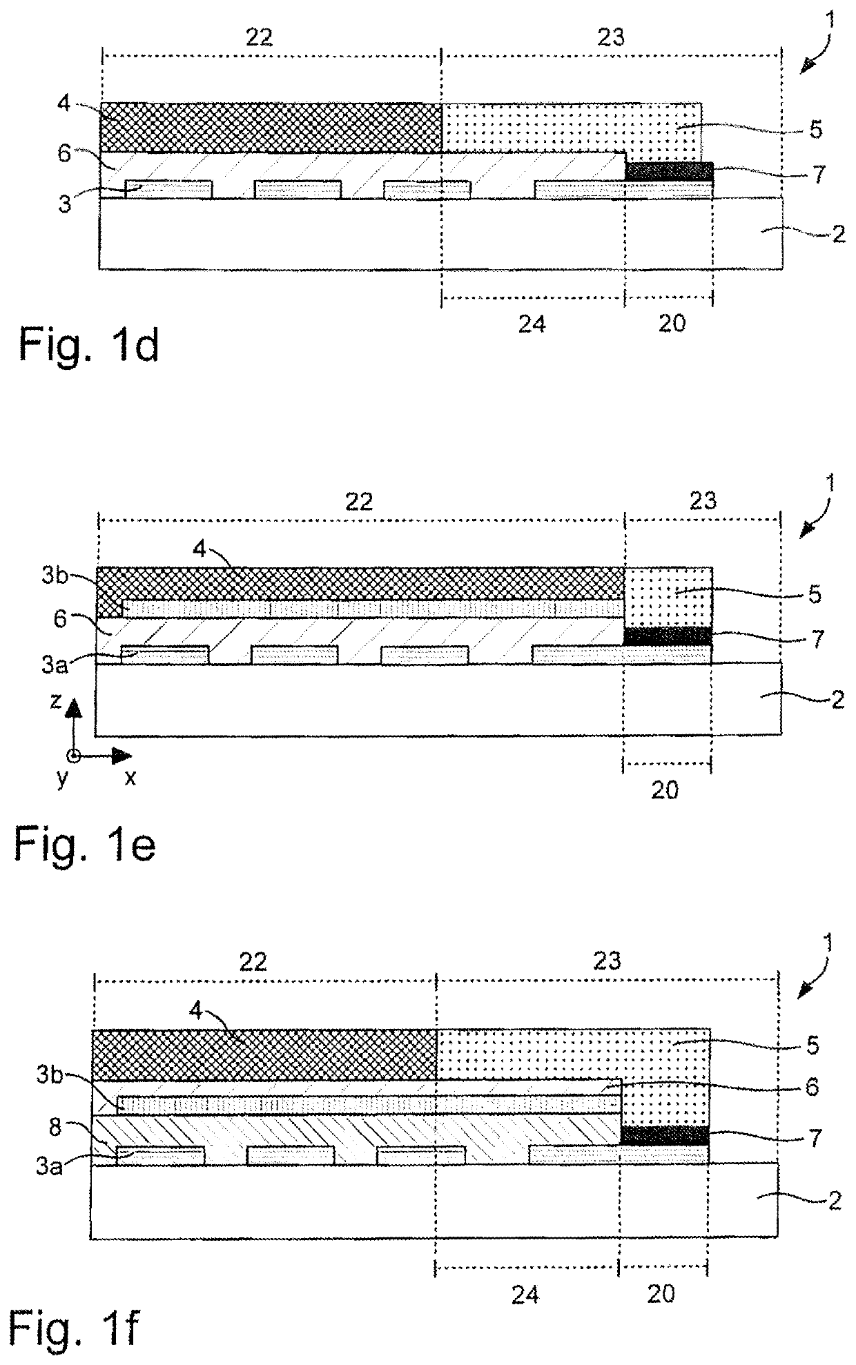
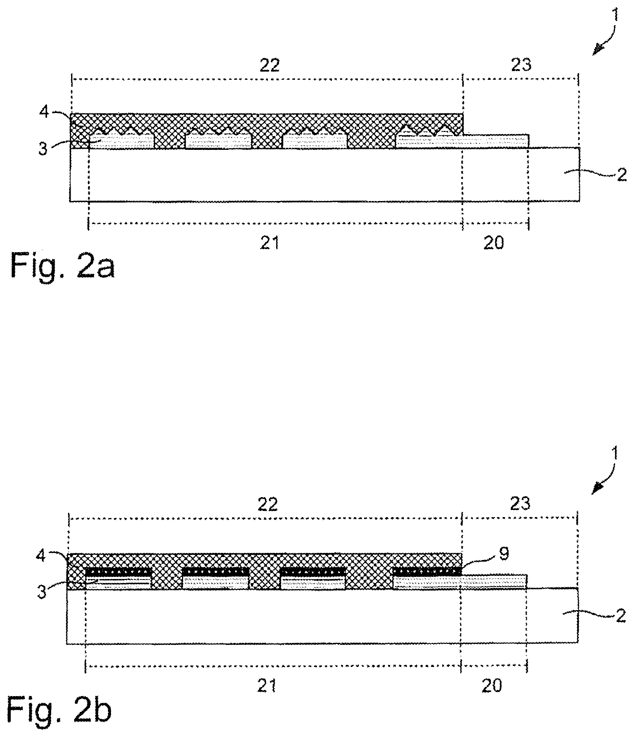
[0253]FIG. 1a shows a film 1 with a carrier substrate 2, an electrically conductive layer 3 and an adhesion-promoting layer 4.

[0254]The carrier substrate 2 is preferably a layer made of PET, PMMA, PC, ABS, PU, glass or fabric. It is also possible for the carrier substrate 2 to be formed from a hybrid material which comprises plastic layers and layers made of fabric, in particular fiber material, such as for example paper, cotton, or other natural or synthetic fibers. The carrier substrate 2 preferably has a layer thickness between 2 μm and 250 μm, preferably between 23 μm and 125 μm. The carrier substrate 2 shown in FIG. 1a is a transparent layer made of PET with a layer thickness of 75 μm.

[0255]By transparent is meant here the property of materials to allow light from the wavelength range visible to the human eye, in particular from the wavelength range between 380 nm and 780 nm, to pass through.

[0256]The electrical conductive layer 3 is preferably a layer made of metal, in particu...


PUM

PropertyMeasurementUnit
widthaaaaaaaaaa
thicknessaaaaaaaaaa
thicknessaaaaaaaaaa

Abstract

A film, a method for producing a film, the use of a film for application to a target substrate as well as a method for producing an electrical functional element. The film here includes a carrier substrate, an adhesion-promoting layer for applying the film to a target substrate, and at least one electrically conductive layer, wherein the at least one electrically conductive layer forms an electrical functional structure in a functional region, wherein the at least one electrically conductive layer forms at least one contacting structure for contacting the electrical functional structure in at least one contacting region, and wherein the adhesion-promoting layer does not cover the at least one contacting region at least in areas when viewed perpendicularly to a plane spanned by the carrier substrate or wherein the adhesion-promoting layer is applied over the whole surface when viewed perpendicularly to a plane spanned by the carrier substrate.

Description

[0001]This application claims priority based on an International Application filed under the Patent Cooperation Treaty, PCT / EP2016 / 078349, filed Nov. 21, 2016, which claims priority to DE102015121195.5, filed Dec. 4, 2015, DE102016101736.1, filed Feb. 1, 2016 and DE102016114638.2, filed Aug. 8, 2016.BACKGROUND OF THE INVENTION[0002]The invention relates to a film, a method for producing a film, the use of a film for application to a target substrate as well as a method for producing an electrical functional element.[0003]Combined input and output devices such as touchscreens, which are also called touch-sensitive screens, have various uses. Thus, for example, the use of touchscreens makes it possible to control a computer program by touching the touchscreen. For this, a touch sensor panel which detects touch is typically arranged on a display element, such as for example a liquid crystal display. The touch sensor panel thus makes it possible to control the image generated by the dis...

Claims


Application Information

Patent Timeline
Patent Type & Authority Patents(United States)
IPC IPC(8): B32B3/00G06F3/041B32B7/14B32B37/06B32B37/12
CPCG06F3/041B32B7/14B32B37/06B32B37/1292B32B2255/205B32B2307/202B32B2309/02B32B2457/208G06F2203/04103G06F2203/04104C09J7/29C09J2301/122C09J2301/16C09J2203/326G06F3/0446C09D127/06C09D133/12C09D175/04C09J7/00C09J127/06C09J133/12C09J175/04G06F3/044
Inventor HEINRICH, MATTHIASHIRSCHFELDER, ANDREASHAHN, MARTINSCHAD, JOHANNES
Owner LEONHARD KURZ STIFTUNG & CO KG
Why Eureka
Try Eureka