Main board and computer apparatus with connectors of both dual in-line package and surface mount technology

a computer and connector technology, applied in the field of main boards, can solve the problems of affecting the signal transmission quality and making the signal inability to be correctly interpreted by the cpu and the memory, and achieve the effect of improving the signal transmission performance of the memory

Active Publication Date: 2021-01-19
WISTRON CORP
View PDF8 Cites 1 Cited by
  • Summary
  • Abstract
  • Description
  • Claims
  • Application Information

AI Technical Summary

Benefits of technology

[0005]In view of the above, the disclosure provides a main board and a computer apparatus in which a DIP connector and a surface mount technology (SMP) connector are applied to reduce at least one via hole, thereby improving signal transmission performance of a memory.
[0026]In light of the foregoing, according to an embodiment, a hybrid connector configuration (i.e., DIP and SMT connectors) is provided, and the via is merely arranged on the DIP connector but not the SMT connector, thereby solving the crosstalk issue to some extent. Given that one via is provided, the overall performance provided in an embodiment here is greater than that achieved by the conventional dual DIP connectors. Moreover, even if the via is removed, the performance provided in an embodiment here is also satisfactory.

Problems solved by technology

Although the conventional structure depicted in FIG. 1 may satisfy the current requirement for mainstream transmission rate (less than 2933 transmission times per second (MT / s)), if the mainstream transmission rate reaches 3200 MT / s in the future, excessive crosstalk derived from parasitic capacitance effect may pose an impact on the vias connected to the two DIP connectors, which greatly affects the signal transmission quality and makes the signal unable to be correctly interpreted by the CPU and the memories.

Method used


Image

  • Main board and computer apparatus with connectors of both dual in-line package and surface mount technology
  • Main board and computer apparatus with connectors of both dual in-line package and surface mount technology
  • Main board and computer apparatus with connectors of both dual in-line package and surface mount technology

Examples


first embodiment

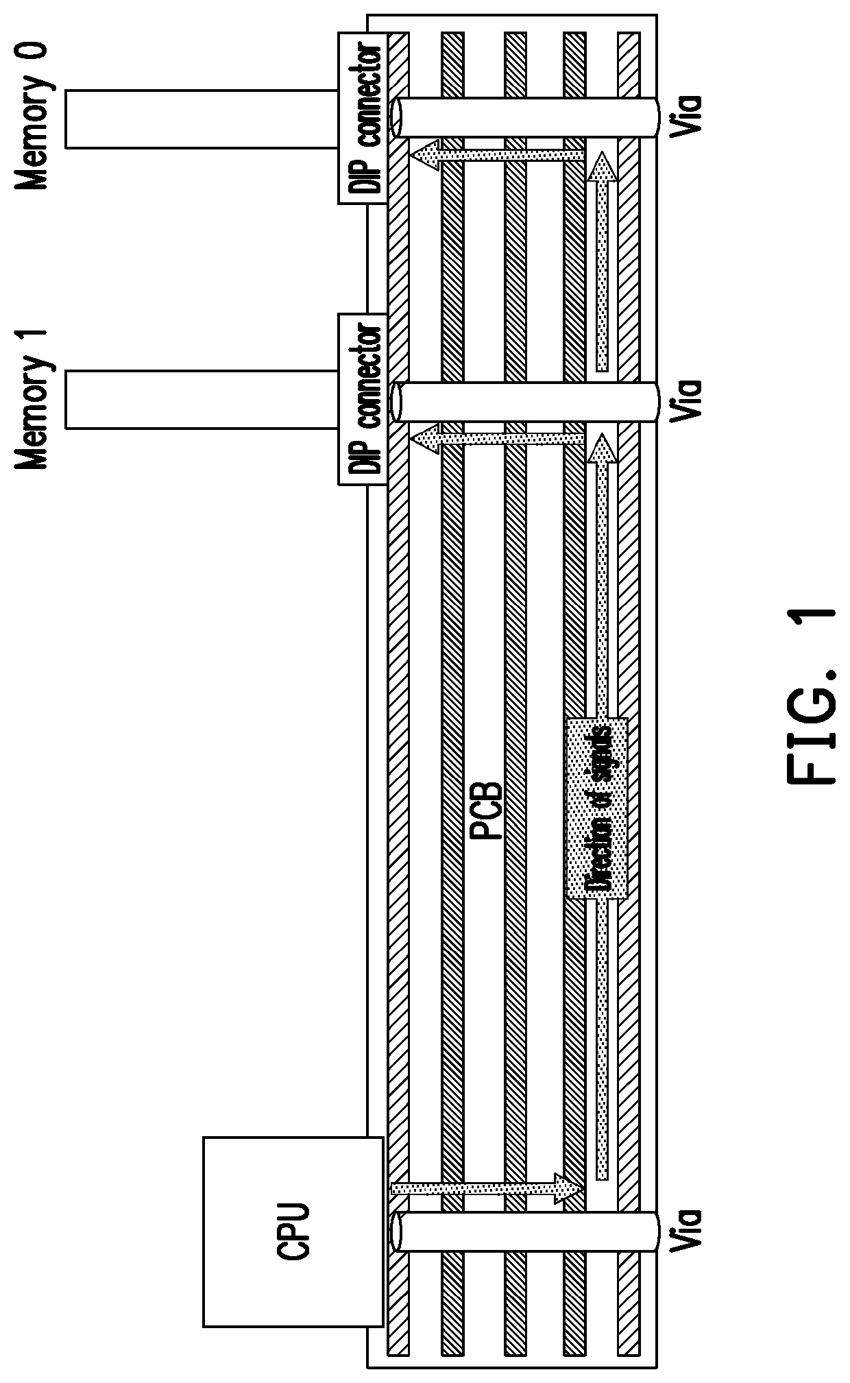
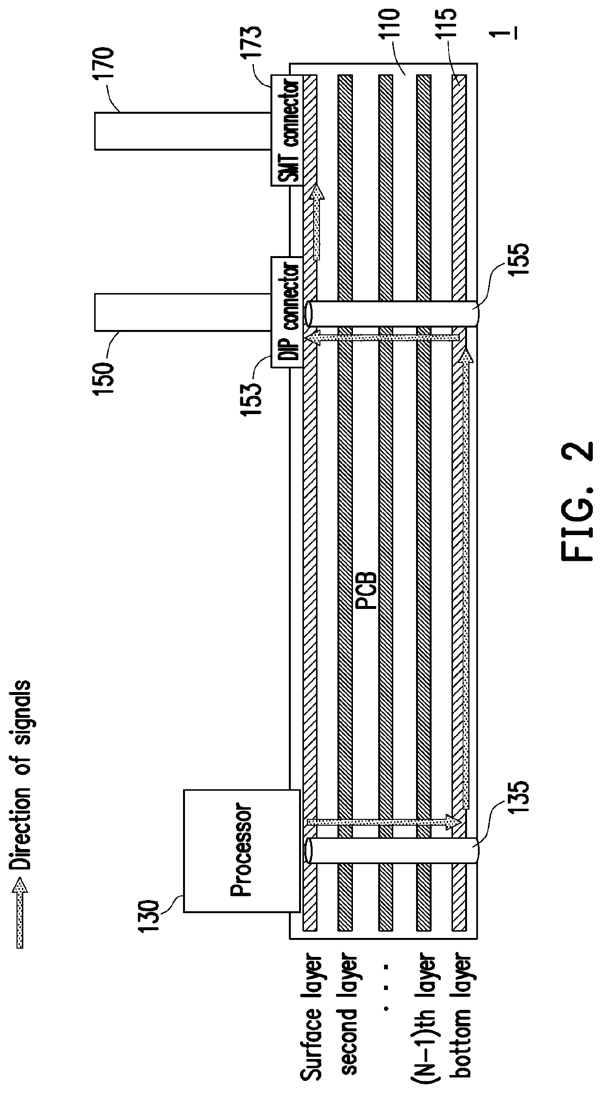
[0036]FIG. 2 is a schematic view of a main board 1 according to the disclosure. With reference to FIG. 2, the main board 1 includes but is not limited to a PCB 110, two vias 135 and 155, a DIP connector 153, and a SMT connector 173.

[0037]The PCB 110 includes multiple layers of circuit substrates, i.e., N layers including the surface layer, the second layer, . . . , the (N−1)th layer, and the bottom layer as shown in the drawings, wherein N is a positive integer greater than 1. The circuit substrates have circuit traces (also referred to as circuits) made of copper or other conductive substance to electrically conduct the soldered electronic components (e.g., resistors, capacitors, inductors, or different types of chips), and the PCB 110 is configured for being electrically connected to the processor 130, the DIP connector 153, and the SMT connector 173.

[0038]The vias 135 and 155 are formed on the PCB 110 (the PCB 110 must first be drilled, and the drilled holes are coated with condu...

second embodiment

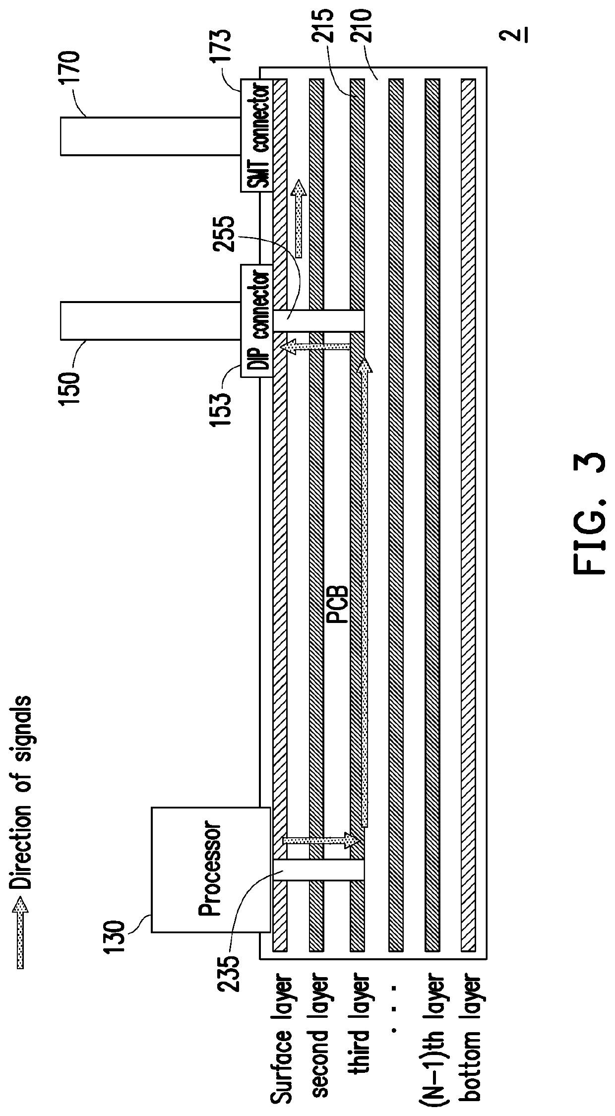
[0043]FIG. 3 is a schematic view of a main board 2 according to the disclosure. With reference to FIG. 3, the main board 2 includes but is not limited to a PCB 210, two vias 235 and 255, a DIP connector 153, and a SMT connector 173.

[0044]Different from the first embodiment, the second embodiment discloses that the signal transmission layer 215 of the PCB 210 for signal transmission related to the memory is located at the third layer (i.e., located between the surface layer and the bottom layer), and the length of the vias 235 and 255 is approximately the distance from the surface layer to the third layer (i.e., shorter than the length of the vias 135 and 155).

third embodiment

[0045]FIG. 4 is a schematic view of a main board 3 according to the disclosure. With reference to FIG. 4, the main board 3 includes but is not limited to a PCB 310, two vias 335 and 355, a DIP connector 153, and a SMT connector 173.

[0046]Different from the first embodiment, the third embodiment discloses that the signal transmission layer 315 of the PCB 310 for signal transmission related to the memory is located at the twelfth layer (i.e., located between the surface layer and the bottom layer), and the length of the vias 335 and 355 is approximately the distance from the surface layer to the twelfth layer (i.e., shorter than the length of the vias 135 and 155).

[0047]Note that the number of layers of circuit substrates in the first, second and third embodiments may be adjusted according to the actual of the user (in consideration of the size of the circuit substrates and whether the length of the circuit trace is sufficient); that is, the signals may be transmitted to the memory th...


PUM


Abstract

A main board and a computer apparatus having the main board are provided. The main board includes a printed circuit board (PCB), a first connector, and a second connector. The PCB is configured for being electrically connected to a processor. The first connector is electrically connected to the PCB in a dual in-line package (DIP) manner, and is configured for a memory to be mounted to the first connector. The second connector is electrically connected to the PCB in a surface mount technology (SMT) manner, and is configured for the memory to be mounted to the second connector. Accordingly, transmission performance of memory signals may be improved.

Description

CROSS-REFERENCE TO RELATED APPLICATION[0001]This application claims the priority benefit of Taiwan application serial no. 107203996, filed on Mar. 28, 2018. The entirety of the above-mentioned patent application is hereby incorporated by reference herein and made a part of this specification.TECHNICAL FIELD[0002]The disclosure relates to a main board; more particularly, the disclosure relates to a main board and a computer apparatus capable of improving transmission performance of a memory.DESCRIPTION OF RELATED ART[0003]A random access memory (RAM) is an important hardware component used by a computer apparatus (e.g., a desktop computer, a notebook computer, a server, etc.) for temporarily storing data. FIG. 1 is a schematic view of a structure of a conventional computer apparatus. With reference to FIG. 1, a main board of the computer apparatus has multiple layers of printed circuit boards (PCBs) having three vertical interconnect accesses (vias) passing through multiple layers of...

Claims


Application Information

Patent Timeline
Patent Type & Authority Patents(United States)
IPC IPC(8): G11C5/04G11C7/10H05K1/18
CPCG11C5/04G11C7/10H05K1/18G11C2207/10H05K2201/10159H05K1/0243H05K2201/10189H05K3/306
Inventor CHANG, YAO-CHUNGHSU, WEN-JUI
Owner WISTRON CORP
Why Eureka
Try Eureka