
Molten target sputtering (MTS) deposition for enhanced kinetic energy and flux of ionized atoms

a technology of kinetic energy and flux, applied in the direction of vacuum evaporation coating, polycrystalline material growth, crystal growth process, etc., can solve the problems of limited sputtering process, achieve increased kinetic energy, increase the flux density of molecules, and increase the energy latency

Active Publication Date: 2021-03-16
NASA
View PDF10 Cites 0 Cited by
  • Summary
  • Abstract
  • Description
  • Claims
  • Application Information

AI Technical Summary

Benefits of technology

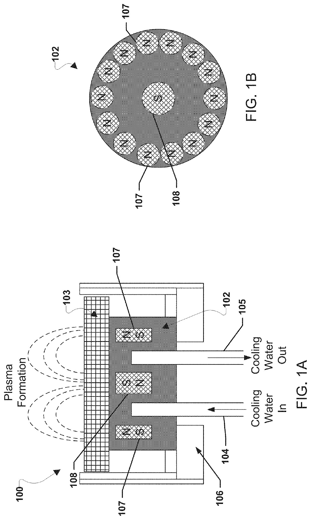
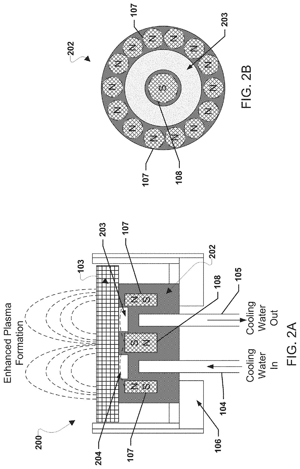
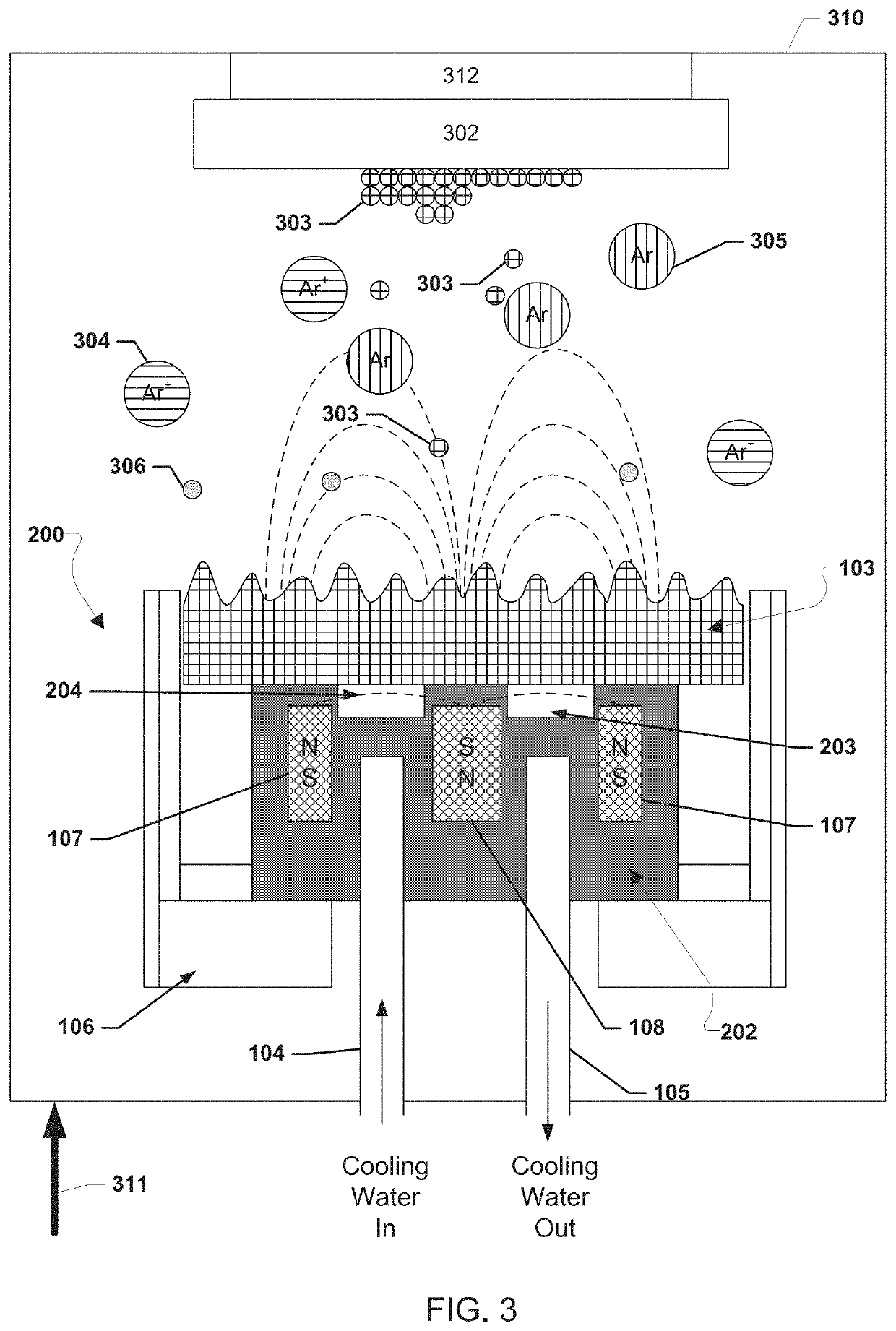
The present invention provides a method and device for Molten Target Sputtering (MTS) that combines the benefits of magnetron sputtering and enhanced evaporation systems. The MTS method and device may increase the energy and kinetic energy of molecules, which can lead to faster and better crystal formation on low temperature substrates. Additionally, the MTS method and device may allow for the growth of a single crystal Si1-xGex film on a substrate heated to less than 500°C. The MTS method and device may also increase the flux density of atomic sputtering and the kinetic energy of the atoms. The MTS method and device may not require the addition of extra systems and may have a ring groove in the surface of a heat sink between magnets that forms a gap during sputtering to reduce heat dissipation and increase the number of detached atoms.

Problems solved by technology

However, since only surface atoms can be sputtered and freed, the sputtering process is limited by low deposition rates and is also limited by low energy carrying sputtered atoms.

Method used


Image

  • Molten target sputtering (MTS) deposition for enhanced kinetic energy and flux of ionized atoms
  • Molten target sputtering (MTS) deposition for enhanced kinetic energy and flux of ionized atoms
  • Molten target sputtering (MTS) deposition for enhanced kinetic energy and flux of ionized atoms

Examples


Embodiment Construction

[0014]It is to be understood that the invention may assume various alternative orientations and step sequences, except where expressly specified to the contrary. It is also to be understood that the specific devices and processes illustrated in the attached drawings, and described in the following specification, are simply exemplary embodiments of the inventive concepts defined in the appended claims. Hence, specific dimensions and other physical characteristics relating to the embodiments disclosed herein are not to be considered as limiting, unless the claims expressly state otherwise.

[0015]To configure a rhombohedral structure of crystal, substrate temperature should be maintained close to or above the melting point of an epitaxial component to deliver sufficient energy to the atoms and molecules from sputter target materials while landing on the substrate. Normally zinc-blende or cubic structure of materials may not be structurally settled as a regular formation of crystal on a ...


PUM

PropertyMeasurementUnit
widthaaaaaaaaaa
temperatureaaaaaaaaaa
depthaaaaaaaaaa

Abstract

Various embodiments provide Molten Target Sputtering (MTS) methods and devices. The various embodiments may provide increases in the kinetic energy, increases in the energy latency, and / or increases in the flux density of molecules for better crystal formation at low temperature operation. The various embodiment MTS methods and devices may enable the growth of a single crystal Si1-xGex film on a substrate heated to less than about 500° C. The various embodiment MTS methods and devices may provide increases in the kinetic energy, increases in the energy latency, and / or increases in the flux density of molecules without requiring the addition of extra systems.

Description

CROSS-REFERENCE TO RELATED PATENT APPLICATION(S)[0001]This patent application claims the benefit of and priority to U.S. Provisional Patent Application No. 62 / 310,216, filed on Mar. 18, 2016, the contents of which is hereby incorporated by reference in its entirety.STATEMENT REGARDING FEDERALLY SPONSORED RESEARCH OR DEVELOPMENT[0002]The invention described herein was made in the performance of work under a NASA contract and by an employee of the United States Government and is subject to the provisions of Public Law 96-517 (35 U.S.C. § 202) and may be manufactured and used by or for the Government for governmental purposes without the payment of any royalties thereon or therefore. In accordance with 35 U.S.C. § 202, the contractor elected not to retain title.BACKGROUND OF THE INVENTION[0003]Sputtering has emerged as one of the major deposition techniques for thin film coating practices in both research and industrial production. Many materials have been successfully deposited using ...

Claims


Application Information

Patent Timeline
Patent Type & Authority Patents(United States)
IPC IPC(8): C23C14/34C30B23/08C23C14/35H01J37/32H01J37/34C30B29/52H01L21/02C23C14/06C30B23/00C30B23/06
CPCC30B23/08C23C14/06C23C14/3414C23C14/3428C23C14/35C30B23/005C30B23/06C30B29/52H01J37/32027H01J37/32082H01J37/32669H01J37/3405H01J37/345H01J37/3414H01J37/3426H01J37/3432H01J37/3435H01J37/3497H01L21/0242H01L21/02532H01L21/02598H01L21/02631
Inventor KIM, HYUN JUNGCHOI, SANG H.
Owner NASA
Learn More