Devices and methods for optical imaging by means of off-axis digital holography

a technology of optical imaging and digital holography, applied in the field of optical imaging devices and methods using off-axis digital holography, can solve the problems of small variations in the amplitude of a light wave used in conventional microscopy, limited sensitivity of the system, and sensitive to the measurement environment, so as to ensure the stability of the device and imaging quality, and ensure the effect of compact holographic imaging

Active Publication Date: 2021-08-24
CENT NAT DE LA RECHERCHE SCI +1
View PDF4 Cites 0 Cited by
  • Summary
  • Abstract
  • Description
  • Claims
  • Application Information

AI Technical Summary

Benefits of technology

[0018]The applicants demonstrated that the original arrangement, in an off-axis holographic imaging device, of an assembly of one or more Bragg gratings to form the reference wave and the signal wave, ensured robustness, compactness of the device and imaging quality. Indeed, the reference wave and the signal wave thus formed directly interfere at the output of the Bragg grating(s), thus avoiding that the device is subjected to external disturbances. Not only do thick Bragg gratings intrinsically generate a spatial low-pass filtering of the deflected wave (reference wave), which contributes to the very good quality of the reconstructed hologram, but in addition, the proposed original arrangement allows an extremely compact holographic imaging device to be formed. The applicants showed that with such an arrangement, the distance between the object and the detection device (sensor) could be reduced to less than 10 centimetres, advantageously less than one centimetre, or even less than a few millimetres.
[0019]According to one or more examples of embodiment, said assembly of one or more thick Bragg gratings comprises at least one first thick Bragg grating with index strata arranged in a first direction, with a first given pitch and at least one second thick Bragg grating with index strata arranged in a second direction, perpendicular to the first direction, with a second given pitch. This arrangement allows to obtain a deflection of the reference wave with respect to the non-deflected signal wave with deflection angles defined in two perpendicular planes.
[0020]According to one or more examples of embodiment, said assembly of one or more thick Bragg grating(s) comprises at least one first thick Bragg grating with multiplexed index strata, having index strata arranged in two perpendicular directions, with a given pitch in each direction. This arrangement also makes it possible to obtain a deflection of the reference wave with respect to the non-deflected signal wave with deflection angles defined in two perpendicular planes.
[0022]The combination of two thick Bragg gratings with multiplexed index strata allows, for thick Bragg gratings of a given thickness, to ensure a greater angular selectivity of the deflected reference wave.

Problems solved by technology

Indeed, in the fields of biology for example, most microscopic objects, such as living cells, are transparent and differ only slightly from their surroundings in terms of absorption or colour, resulting in very small variations in the amplitude of a light wave used in conventional microscopy.
These systems, which allow the skilled person to create Gabor holograms, are however limited in sensitivity due to the spatial superposition of the useful signal ESER* (where * represents the complex conjugation) with the other interference terms in the interferogram.
The device illustrated in FIG. 1B has the disadvantage, however, of being sensitive to the measurement environment; simple disturbances of the ambient air or vibrations can disturb the reference beam and therefore the measurement.

Method used


Image

  • Devices and methods for optical imaging by means of off-axis digital holography
  • Devices and methods for optical imaging by means of off-axis digital holography
  • Devices and methods for optical imaging by means of off-axis digital holography

Examples


Embodiment Construction

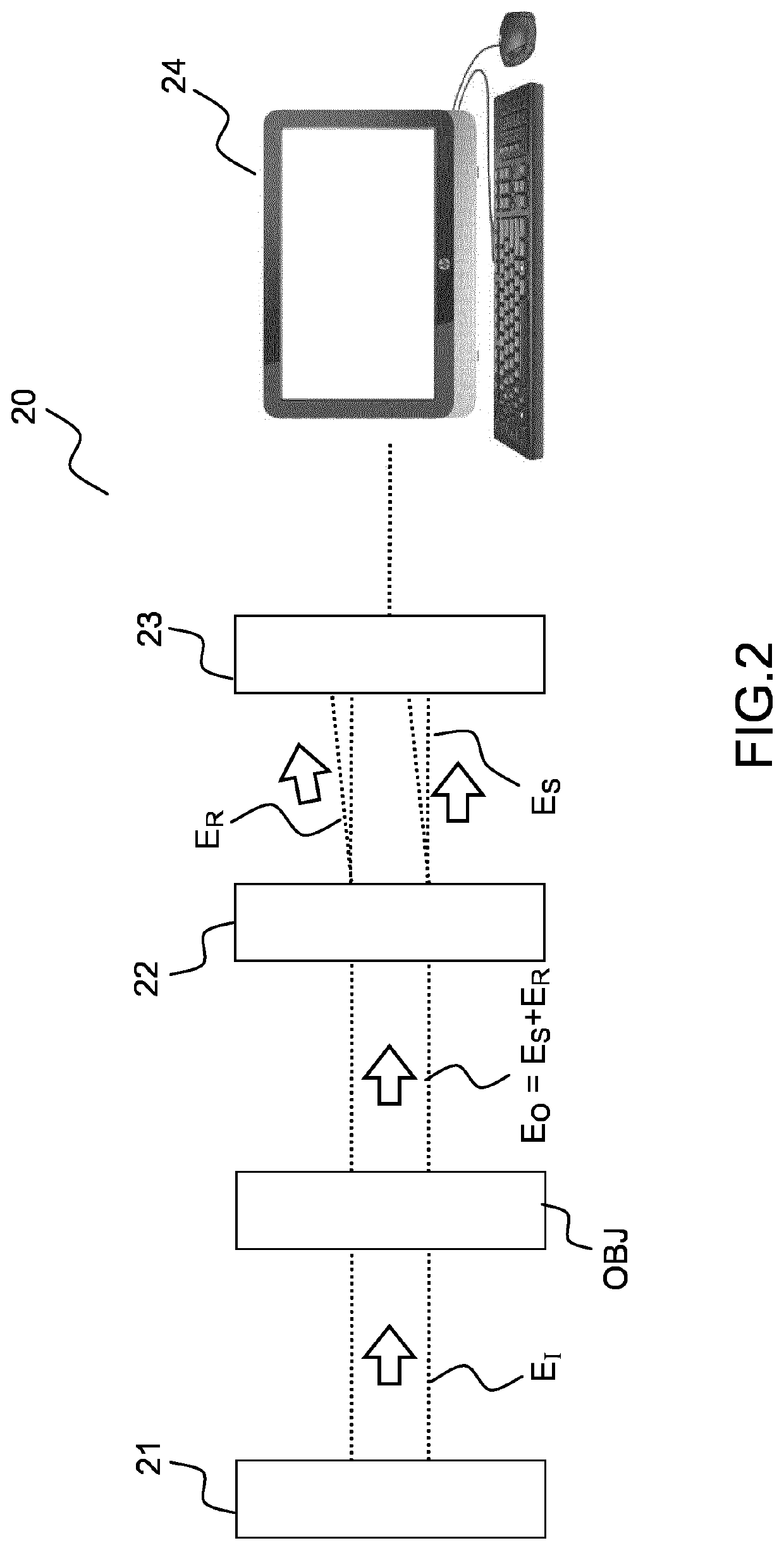
[0038]FIG. 2 represents a diagram of an imaging device 20 example for an object OBJ according to this description. The object is for example a biological sample, for example a culture of living cells, or a material for microelectronics (semiconductor, glass, mirror).

[0039]The imaging device 20 includes a light source 21 adapted for emitting an illumination wave of the object OBJ, whose the electromagnetic field is noted EI. Although represented in transmission in FIG. 2, the illumination of the object can be done in reflection, for example when the object is a semiconductor, glass, or mirror. The light source is for example a laser, a super luminescent diode (or SLD), an electroluminescent diode (or LED according to the abbreviation of the Anglo-Saxon expression “Light-Emitting Diode”).

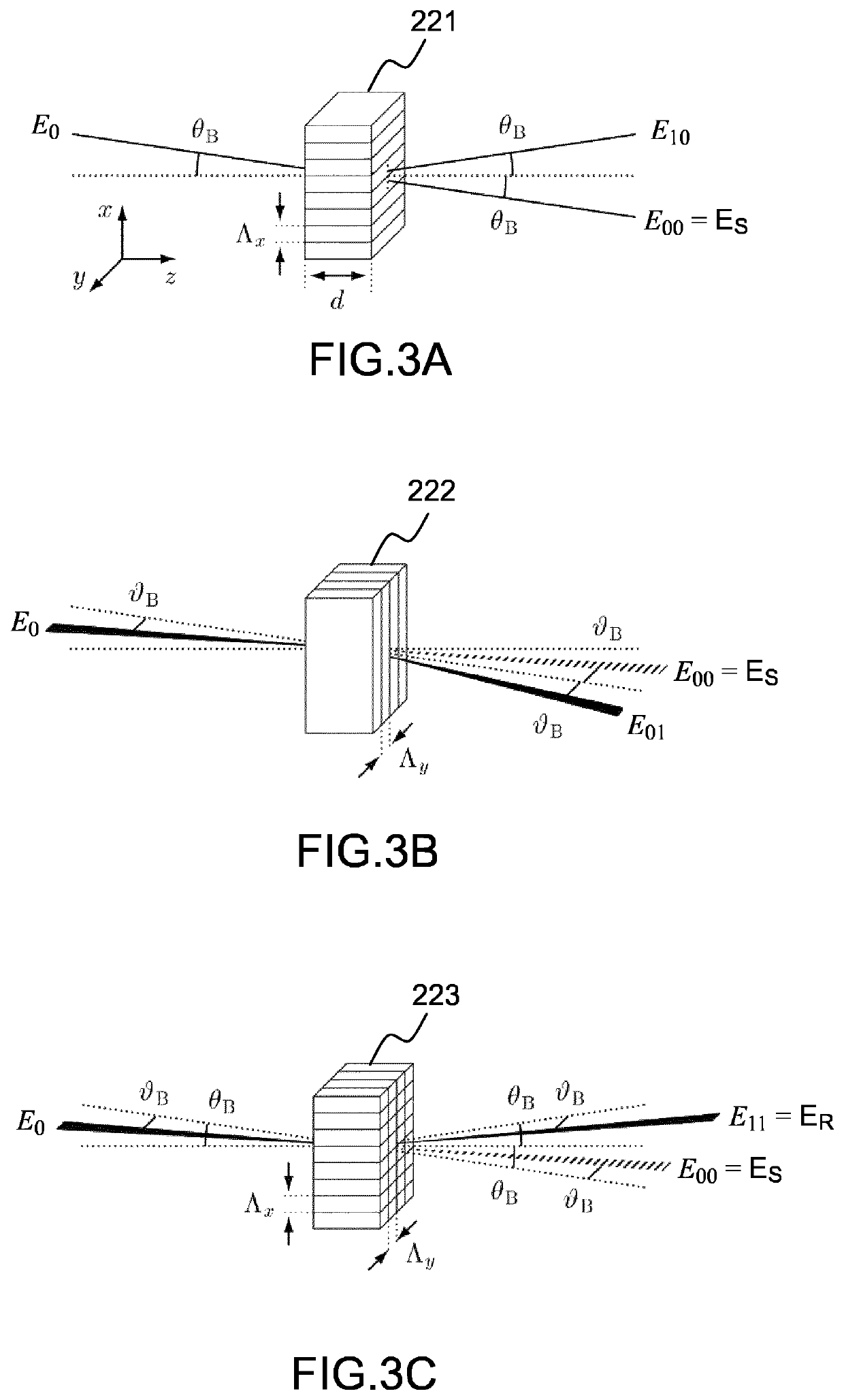
[0040]The imaging device 20 also includes an assembly 22 of one or more thick Bragg gratings to receive a wave coming from the object, with an electromagnetic field EO. The wave coming from the object...


PUM


Abstract

According to one aspect, the invention concerns an optical imaging device (20) for an object (OBJ) by off-axis holography comprising a light source (21) adapted for emitting an illumination wave (EI) on the object, in transmission or reflection, and an assembly formed by one or more thick Bragg gratings (22) for receiving a wave (EO) coming from the object thus illuminated and for deflecting a first component (ER) of the wave coming from the object, called the reference wave, and to allow a second component (ES) of the wave coming from the object, called the signal wave, to pass without deflection in such a way that the deflected reference wave presents predetermined deflection angles with respect to the non-deflected signal wave defined in two perpendicular planes. The imaging device according to the first aspect further comprises a two-dimensional detection device (23) for acquiring an interferogram resulting from the interference between said deflected reference wave and said signal wave and a computing unit for determining, from said interferogram, an amplitude and phase distribution of the signal wave in the plane of the object (hologram).

Description

STATE OF THE ARTTechnical Field of the Invention[0001]This invention concerns optical imaging devices and methods using off-axis digital holography and applies in particular to microscopic imaging, in particular of transparent or reflective objects.State of the Art[0002]Phase contrast microscopy developed as early as the 1940s for the observation of transparent microscopic objects. Indeed, in the fields of biology for example, most microscopic objects, such as living cells, are transparent and differ only slightly from their surroundings in terms of absorption or colour, resulting in very small variations in the amplitude of a light wave used in conventional microscopy. Phase contrast microscopy allows the detection of variations in the refractive index within the object to form an image. In particular, interferometric techniques based on interference between a light beam transmitted or reflected by the object and a reference light beam have provided access to quantitative measureme...

Claims


Application Information

Patent Timeline
Patent Type & Authority Patents(United States)
IPC IPC(8): G03H1/04G03H1/00
CPCG03H1/041G03H1/0443G03H2001/005G03H2001/0445G03H1/0248G03H2210/12G03H2222/45G03H2223/23
Inventor ATLAN, MICHAELHUIGNARD, JEAN-PIERRE
Owner CENT NAT DE LA RECHERCHE SCI
Why Eureka
Try Eureka