Display panel having a nano-stack layer

a display panel and nano-stack technology, applied in the field of displays, can solve the problems of poor contrast of the quantum dot light-emitting diode display panel b>90/b> in a dark state, and achieve the effects of preventing the influence of ambient light on the device, reducing light loss, and improving light output efficiency

Active Publication Date: 2021-09-14
SHENZHEN CHINA STAR OPTOELECTRONICS SEMICON DISPLAY TECH CO LTD
View PDF39 Cites 0 Cited by
  • Summary
  • Abstract
  • Description
  • Claims
  • Application Information

AI Technical Summary

Benefits of technology

[0006]An object of the present invention is to provide a display panel to overcome problems of conventional quantum dot light-emitting diode display panels, such as low light output efficiency, low brightness, and poor contrast in a dark state.
[0017]The present invention relates to a display panel. On one hand, by using at least one first nano-stack provided in the encapsulation layer to reflect light, specifically red and / or green light, emitted from the color filter substrate, the present invention can reduce light loss of the red light quantum dot conversion unit and the green light quantum dot conversion unit due to scattering, thereby improving light output efficiency. On the other hand, by using at least one second nano-stack layer provided in the buffer layer to reflect light, specifically blue light, emitted from the light-emitting substrate, not only influence on devices from ambient light can be prevented, but also a reflected light path can be formed between the second nano-stack layer and the second electrodes, so that blue light can enter the quantum dot photoconversion layer multiple times and be used, and a utilization efficiency of blue light can be improved, thereby overcoming problems of conventional quantum dot light-emitting diode display panels, such as low light output efficiency, low brightness, and poor contrast in a dark state.

Problems solved by technology

Furthermore, because of influence of ambient light, a contrast of the quantum dot light-emitting diode display panel 90 in a dark state is poor.

Method used


Image

  • Display panel having a nano-stack layer
  • Display panel having a nano-stack layer
  • Display panel having a nano-stack layer

Examples


embodiment 1

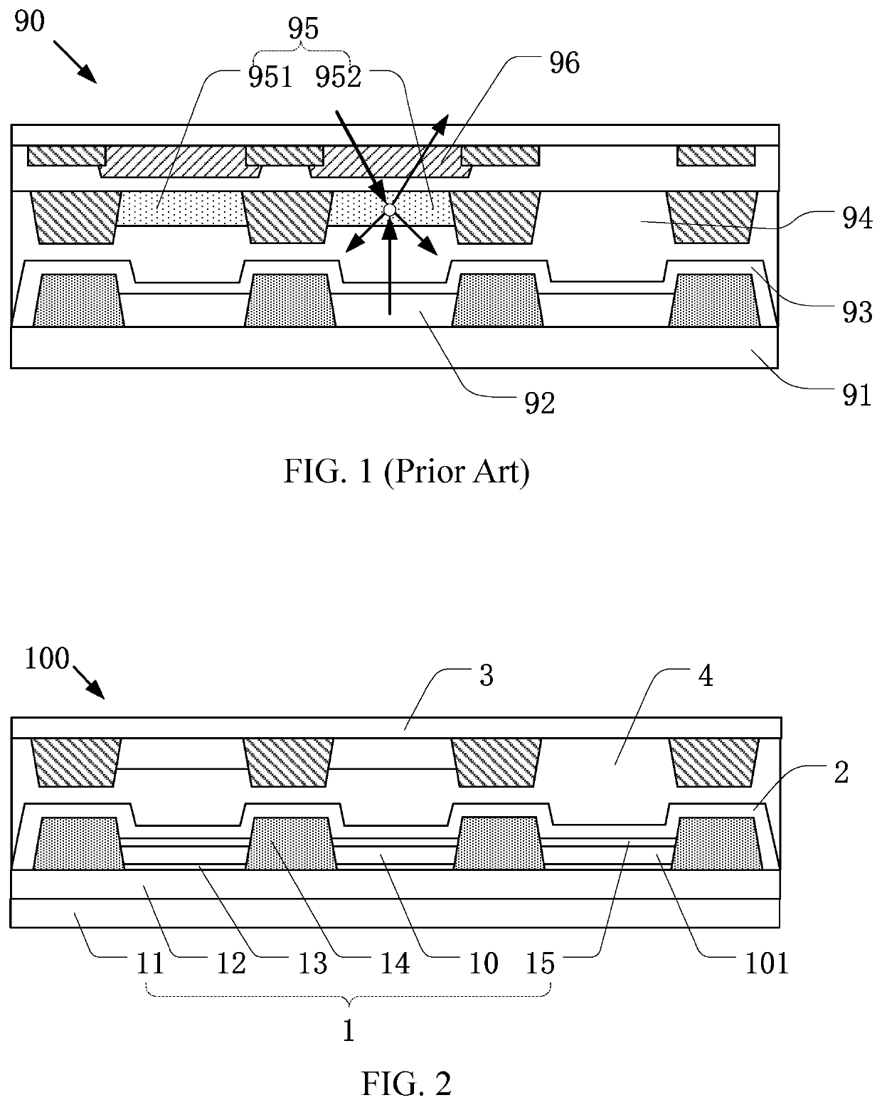
[0030]As shown in FIGS. 2 and 3, the present invention provides a display panel 100 including a light-emitting substrate 1, an encapsulation layer 2, and a color filter substrate 3. The light-emitting substrate 1 includes a light-emitting layer 10 for providing a light source. Preferably, light emitted by the light-emitting layer 10 includes blue light. The encapsulation layer 2 is disposed on the light-emitting substrate1 and has a stack structure composed of inorganic layers and organic layers, thereby to prevent moisture and oxygen intrusion. The color filter substrate 3 is disposed opposite to the light-emitting substrate 1. The encapsulation layer 2 includes at least a first nano-stack layer 21 for reflecting light emitted from the color filter substrate 3. The first nano-stack layer 21 includes a first inorganic layer 211 and a first organic layer 212 disposed in a stack arrangement, wherein the first organic layer 212 has a refractive index less than a refractive index of the...

embodiment 2

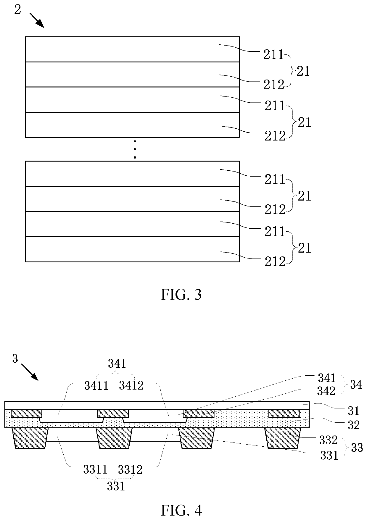
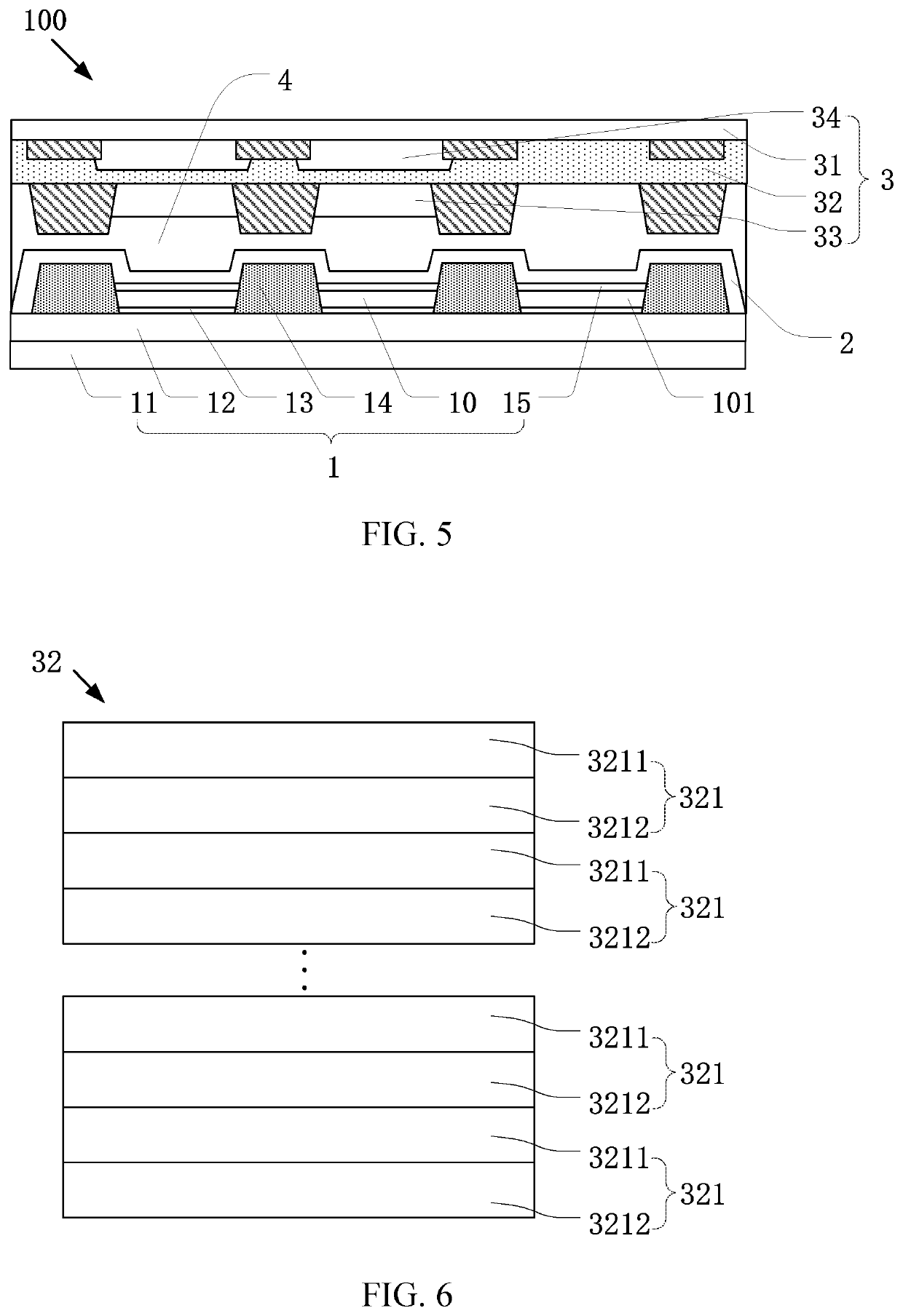
[0038]As shown in FIGS. 4, 5, and 6, the second embodiment includes all the technical features of the first embodiment. A difference from the first embodiment lies in that the color filter substrate 3 in the second embodiment includes a base layer 31, a buffer layer 32, and a quantum dot photoconversion layer 33. The buffer layer 32 is disposed on the base layer 31 and includes at least a second nano-stack layer 321 for reflecting light emitted from the light-emitting substrate 1. The quantum dot photoconversion layer 33 is disposed on a surface of the buffer layer 32 facing the light-emitting substrate 1. The second nano-stack layer 321 includes a second inorganic layer 3211 and a second organic layer 3212 disposed in a stack arrangement, and the second organic layer 3212 has a refractive index less than a refractive index of the second inorganic layer 3211.

[0039]As shown in FIG. 6, in this embodiment, when the buffer layer 32 has only one second nano-stack layer 321, the refractiv...

embodiment 3

[0044]As shown in FIG. 7, the third embodiment includes all the technical features of the second embodiment. A difference from the second embodiment lies in that there is no color filter layer 34 provided in the third embodiment, and remains only the quantum dot photoconversion layer 33 having a thickness between 20 nm and 100 nm, so that the color filter layer 34 can be left out, thereby increase brightness of the panel, and at the same time preventing ambient light from causing degradation of the quantum dot photoconversion unit 331 and the light-emitting layer 10.

[0045]The principle of increasing the brightness is that the color filter layer 34 functions to filter out excess light of other colors to obtain pure monochromatic light. At present, a thickness of the quantum dot photoconversion layer 33 can be reached at about 10 nm, and the color film layer 34 needs to be fabricated. When the quantum dot photoconversion layer 33 is relatively thick, for example, 20 nm or more, excess...


PUM

PropertyMeasurementUnit
thicknessaaaaaaaaaa
thicknessaaaaaaaaaa
thicknessaaaaaaaaaa

Abstract

A display panel includes a light-emitting substrate, an encapsulation layer, and a color filter substrate. The encapsulation layer includes at least a first nano-stack layer for reflecting light emitted from the color filter substrate. The first nano-stack layer includes a first inorganic layer and a first organic layer disposed in a stack arrangement, and the first organic layer having a refractive index less than a refractive index of the first inorganic layer. By using at least one first nano-stack provided in the encapsulation layer to reflect red and / or green light emitted from the color filter substrate, the present invention can reduce light loss of the red light quantum dot conversion unit and the green light quantum dot conversion unit due to scattering, and improve light output efficiency.

Description

BACKGROUND OF INVENTION1. Field of Invention[0001]The present invention relates to a technical field of displays, and particularly to, a display panel.2. Related Art[0002]Quantum dot light-emitting diode (QD-OLED) technology is a display technology that combines electroluminescent diodes and quantum dot photoluminescence. QD-OLED technology uses electroluminescent diodes to generate blue light to excite red / green quantum dots to form a full-color display. It has excellent performance, such as wide color gamut and wide viewing angles, and is considered a potential technology for large-sized organic light-emitting diodes (OLEDs).[0003]FIG. 1 shows a schematic structural view of a quantum dot light-emitting diode display panel. The quantum dot light-emitting diode display panel includes an array substrate 91, a blue electroluminescent diode 92, an encapsulation layer 93, an adhesive filled layer 94, a quantum dot photoconversion layer 95, and a color film layer 96 all sequentially stac...

Claims


Application Information

Patent Timeline
Patent Type & Authority Patents(United States)
IPC IPC(8): H01L51/52H01L51/50H01L27/32G02F1/133G02F1/1335
CPCH01L51/5237H01L27/322H01L51/502G02F1/133514H01L51/5253H01L51/5256H01L2251/301H10K59/38H10K50/8445H10K50/856H10K50/84H10K50/115H10K50/844H10K2102/00
Inventor LI, YUANYUAN
Owner SHENZHEN CHINA STAR OPTOELECTRONICS SEMICON DISPLAY TECH CO LTD
Why Eureka
Try Eureka