Analog-to-digital converter with auto-zeroing residue amplification circuit

Active Publication Date: 2021-11-16
ANALOG DEVICES INC
View PDF9 Cites 1 Cited by
  • Summary
  • Abstract
  • Description
  • Claims
  • Application Information

AI Technical Summary

Benefits of technology

The patent describes an improved auto-zeroing residue amplifier that can cancel out non-zero offsets in the amplification process. The amplified residue value is observed in two phases, which results in a relatively higher level of signal compared to a noise level. This relatively lower noise level allows for the implementation of analog-to-digital converters with reduced noise-and-power operation. Overall, the technical effect is improved amplification with reduced noise and improved performance.

Problems solved by technology

ADCs and other circuits may be designed aiming for a constant-zero offset, but imperfections of a manufacturing process, mismatch of nominally-identical semiconductor devices, atom-level charge mobility, etc. may cause a circuit's offset to be potentially non-zero and it may drift with respect to parameters such as time, temperature, and / or supply voltage.
However, legacy AZ circuits may increase a level of broadband noise, which is detrimental when low noise and low power is also desired.
A power consumption of a precision ADC may have to be increased to reduce noise to an acceptable level when an AZ circuit is used.
For comparison, a non-auto-zeroing residue amplifier may provide a relatively lower / better noise-and-power operation, but its offset stability may be relatively poor.

Method used


Image

  • Analog-to-digital converter with auto-zeroing residue amplification circuit
  • Analog-to-digital converter with auto-zeroing residue amplification circuit
  • Analog-to-digital converter with auto-zeroing residue amplification circuit

Examples


example implementations

[0084]The following examples are provided by way of illustration.

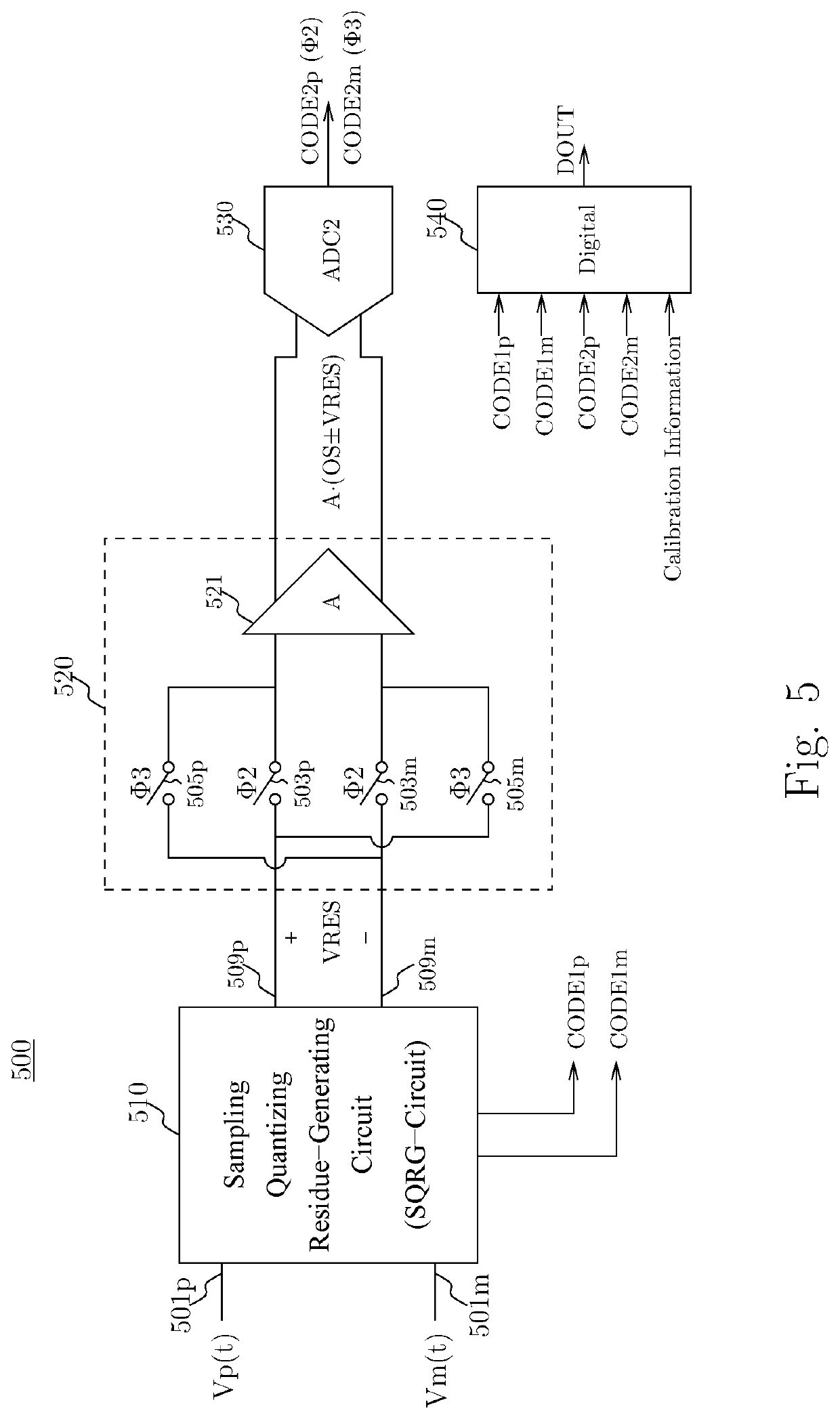
[0085]Example 1 may include an analog-to-digital converter (ADC) circuit for receiving an analog input value and providing a digital output code to represent the analog input value, the ADC circuit comprising a sampling-quantizing-residue-generating (SQRG) circuit configured to receive the analog input value and to provide a first digital code derived at least in part from the analog input value; the SQRG circuit further configured to provide an analog residue value derived at least in part from the analog input value and the first code, an auto-zeroing residue amplification circuit configured to receive and amplify the analog residue value and to provide a first and a second observation of the amplified analog residue value, a quantizer circuit configured to derive a second code to represent a combination of at least the first and second observations of the amplified analog residue value, and a digital circuit configu...


PUM


Abstract

Disclosed herein are some examples of analog-to-digital converters (ADCs) that can perform auto-zeroing with amplifying a signal for improvement of a signal-to-noise ratio. The ADCs may produce a first digital code to represent an analog input signal and a second digital code based on a residue from the first digital code, and may combine the first digital code and the second digital code to produce a digital output code to represent the analog input signal. The ADC may utilize a first observation and a second observation of an analog residue value representing the residue to produce the second digital code.

Description

FIELD OF THE DISCLOSURE[0001]This disclosure relates in general to the field of electronic circuits, and more particularly, though not exclusively, to a system and method for data conversion.BACKGROUND[0002]Analog signals and / or values can be produced in various kinds of circuit elements, such as signal generators, sensors, and antennas. However, there can be many instances where having digital signals or values can be beneficial, such as for a processing or storing of the signals or values. To utilize the benefits of having a digital signal or value when an analog signal or value has been produced, analog-to-digital converters (ADCs) have been developed to convert the analog signal or value into a digital signal or value.[0003]A signal may be a time-based sequence of values. A digital value may be represented by a code. A name of a code (for example, CODE1) may refer to a digital value represented by the code. Some (but not all) digital values may be represented by codes using bina...

Claims


Application Information

Patent Timeline
IPC IPC(8): H03M1/10H03M1/42H03M1/44
CPCH03M1/1023H03M1/42H03M1/44H03M1/08H03M1/0607H03M1/442H03M1/466H03F3/45475H03F3/38H03M1/38H03M1/46H03M1/124H03F3/005
Inventor STEENSGAARD-MADSEN, JESPERTHOMAS, ANDREW
Owner ANALOG DEVICES INC
Why Eureka
Try Eureka