Integrated circuit device having clock signal output circuit

Inactive Publication Date: 2005-09-22
DENSO CORP
View PDF8 Cites 4 Cited by
  • Summary
  • Abstract
  • Description
  • Claims
  • Application Information

AI Technical Summary

Benefits of technology

[0021] In this case, the fluctuation in supply voltage caused by the internal circuit propagates to the clock signal output circuit side. As a result, the supply voltage of the clock signal output circuit is varied as well. Consequently, the delay times of delay gates constituting the ring oscillator vary according to supply voltage fluctuation. Therefore, the frequency of the oscillating operation in the ring oscillator varies. As a result, the frequency of the multiplied cl

Problems solved by technology

Therefore, when internal power supply stabilized by an internal power supply generation circuit is supplied both to a multiplication circuit and to the internal circuit, a problem arises.
However, the technologies according to the prior arts do not give consideration to this problem at all, and with these technologies, occurrences of jitter effect due to fluctuation in internal supply voltage cannot be avoided.
When a clock si

Method used


Image

  • Integrated circuit device having clock signal output circuit
  • Integrated circuit device having clock signal output circuit
  • Integrated circuit device having clock signal output circuit

Examples


Example

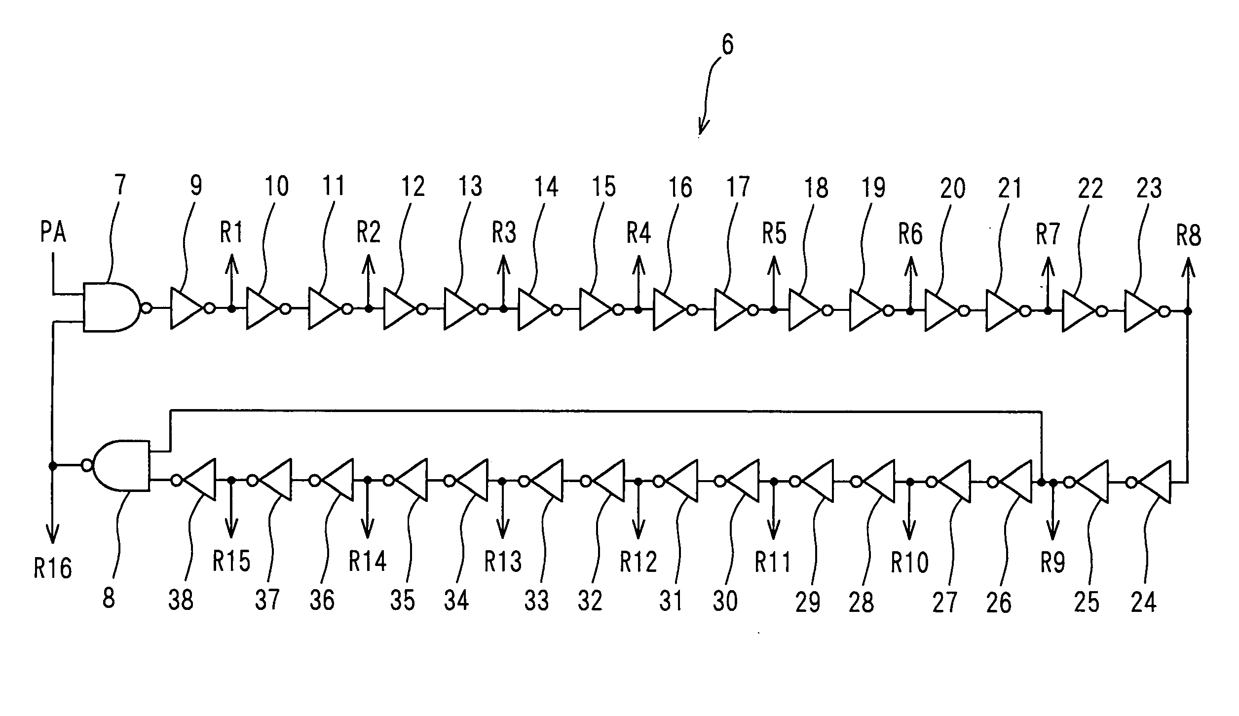
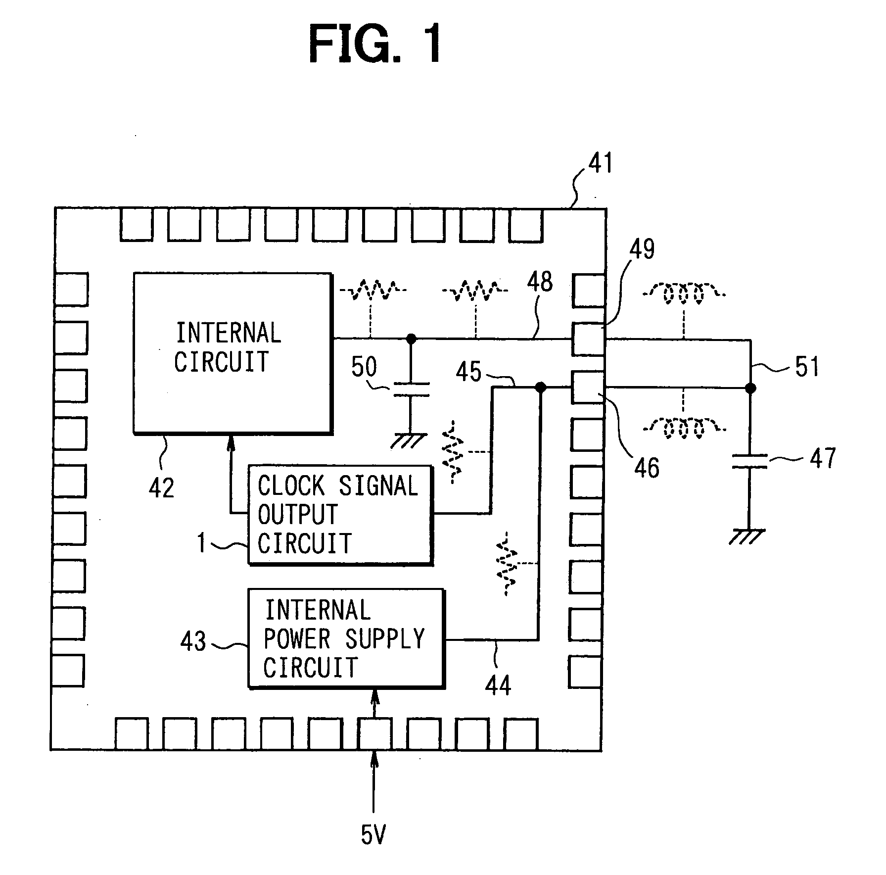
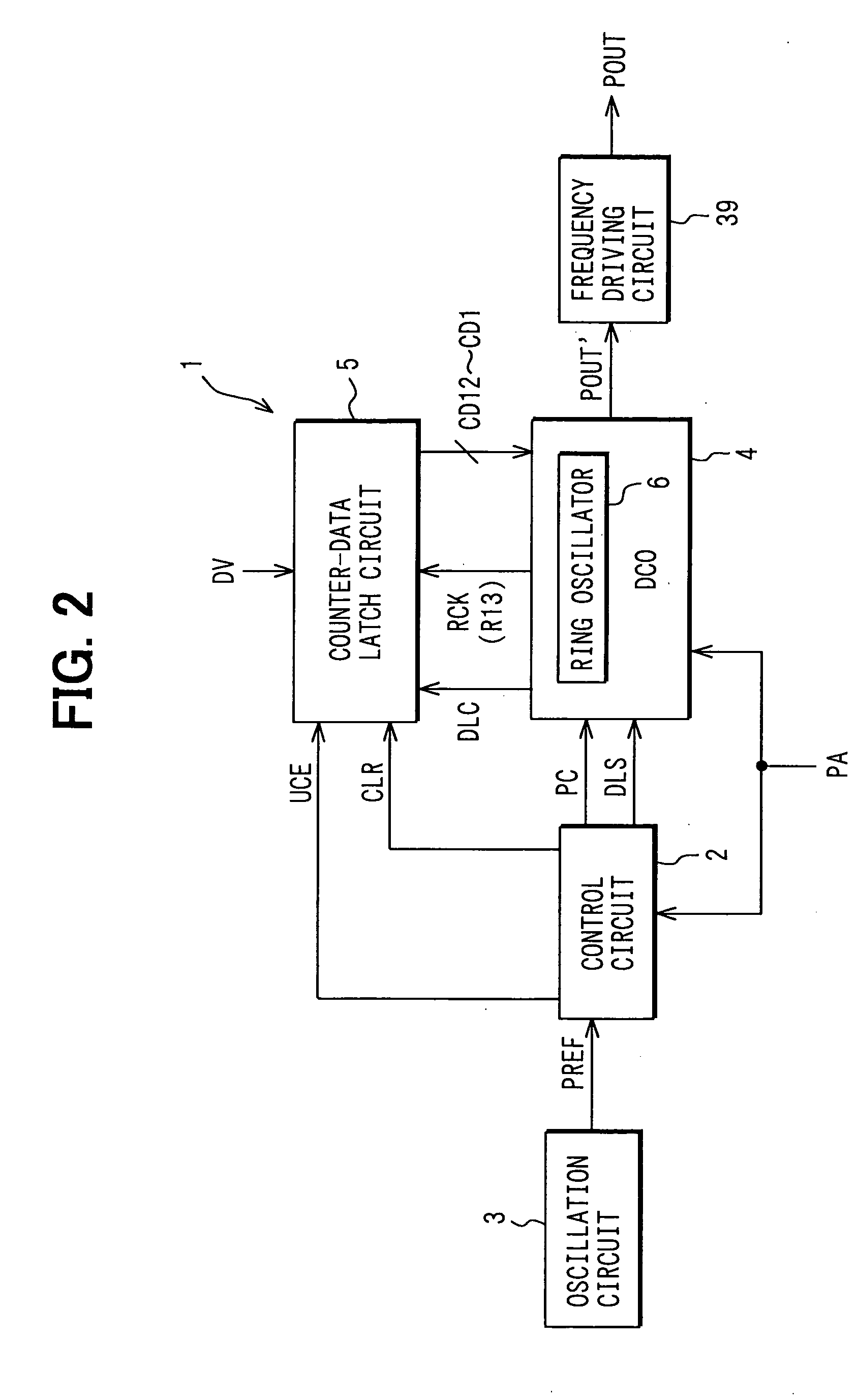
[0039] Hereafter, description will be given to a first embodiment of the present invention with reference to FIG. 1 to FIG. 8. FIG. 2 is a functional block diagram showing the general constitution of a clock signal output circuit 1 constructed of DPLL. (For detailed description of the constitution, refer to Japanese Unexamined Patent Publication No. H8-265111 (which corresponds to U.S. Pat. No. 5,789,985) or Japanese Unexamined Patent Publication No. 2000-357947.) A control circuit 2 is supplied with a reference clock signal PREF outputted from an oscillation circuit 3. The control circuit 2 has a state machine incorporated therein. The control circuit 2 is so designed as to output various control timing signals to DCO (i.e., Digital Controlled Oscillator) 4 and a counter-data latch circuit 5 based on a state counter outputted form the state machine.

[0040] The DCO 4 provides a ring oscillator 6 therein. As illustrated in FIG. 3 as an example, the ring oscillator 6 is so constructed...

Example

[0070]FIG. 9 illustrates a second embodiment of the present invention. In FIG. 9, the same members as in the first embodiment will be marked with the same reference numerals, and the description of such members will be omitted. Hereafter, description will be given only to differences between them. In a one-chip microcomputer (integrated circuit device) 52 according to the second embodiment, the power wiring 45 of the clock signal output circuit 1 is connected to the vicinity of the power output terminal of the internal power supply generation circuit 43. The other aspects of the constitution are the same as those of the first embodiment.

[0071] In the second embodiment constructed as mentioned above, the impedance of wiring between the capacitor connection terminal 46 and the junction point between the power wirings 44 and 45 is increased from the viewpoint of the clock signal output circuit 1. Therefore, the effect of the low-pass filter is further enhanced, and fluctuation in supp...

Example

Third Embodiment

[0080]FIG. 10 schematically illustrates the constitution of a one-chip microcomputer 241 according to a third embodiment of the present invention mounted with the clock signal output circuit 1. The micro 241 is constructed by mounting the clock signal output circuit 1 and an internal circuit 242 over a semiconductor substrate. The internal circuit 242 is supplied with a multiplied clock signal outputted by the clock signal output circuit 1 and is thereby operated. The internal circuit 242 includes, for example, a CPU 243, a ROM 244, a RAM 245, a timer 246, an I / O logic portion 47, and the like. (These elements are strictly for example purposes.)

[0081] The micro 241 is externally supplied with 5V power VDD. A power wiring 248 is routed in the micro 241 so that this power is supplied to the internal circuit 242 first and then to the clock signal output circuit 1. A ground-side wiring 249 is routed similarly with the power wiring 248.

[0082] Next, description will be ...


PUM


Abstract

Integrated circuit device includes: a wiring; a clock signal output circuit including a ring oscillator; an internal circuit; an internal power supply generation circuit for supplying an electric power to the clock signal output circuit and to the internal circuit on the basis of a power supplied from an external circuit; and a capacitor connection terminal. The internal power supply generation circuit supplies the electric power to the ring oscillator through the wiring connecting between the internal power supply generation circuit and the capacitor connection terminal. The internal power supply generation circuit supplies the electric power to the internal circuit through the wiring connecting to the capacitor connection terminal.

Description

CROSS REFERENCE TO RELATED APPLICATIONS [0001] This application is based on Japanese Patent Applications No. 2004-78247 filed on Mar. 18, 2004, and No. 2004-82580 filed on Mar. 22, 2004, the disclosures of which are incorporated herein by reference. FIELD OF THE INVENTION [0002] The present invention relates to an integrated circuit device having a clock signal output circuit. BACKGROUND OF THE INVENTION [0003] Recently, operating clock frequencies have been increased in integrated circuit devices such as microcomputers. For this reason, the following constitution is frequently adopted: a clock multiplication circuit constructed using a PLL (i.e., Phase Locked Loop) circuit is incorporated in an integrated circuit device; and externally supplied clock signals are internally multiplied, and supplied to CPU and the like. Some of such clock multiplication circuits are so constructed that multiplied clock signals are generated and outputted by digital PLL (i.e., DPLL) operation using a ...

Claims


Application Information

Patent Timeline
IPC IPC(8): G06F1/04G06F1/26H03B1/00H03K3/03
CPCG06F1/04H03K3/0315G06F1/26
Inventor MISAWA, KATSUTOYOISHIKAWA, YASUYUKISUZUKI, AKIRATESHIMA, YOSHINORIISHIHARA, HIDEAKI
Owner DENSO CORP
Why Eureka
Try Eureka