Active wafer probe

Inactive Publication Date: 2005-06-30
FORMFACTOR BEAVERTON INC
View PDF99 Cites 14 Cited by
  • Summary
  • Abstract
  • Description
  • Claims
  • Application Information

AI Technical Summary

Benefits of technology

[0006] To achieve improved spatial conformance between the tip conductors of a probe and an array of non-planar device pads or surfaces, several high-frequency probing assemblies have been developed. Such assemblies are described, for example, in Drake et al. U.S. Pat. No. 4,894,612; Coberly et al. U.S. Pat. No. 4,116,523; and Boll et al. U.S. Pat. No. 4,871,964. Similarly, such probing assembly is designed to present a typical transmission line impedance, such as 50 ohms, to the device under test. The Drake et al. probing assembly includes a substrate on the underside of which are formed a plurality of conductive traces which collectively form a coplanar transmission line. However, in one embodiment shown in Drake et al., the tip end of the substrate is notched so that each trace extends to the end of a separate tooth and the substrate is made of moderately flexible nonceramic material. The moderately flexible substrate permits, at least to a limited extent, independent flexure of each tooth relative to the other teeth so as to enable spatial conformance of the trace ends to slightly non-planar contact surfaces on a device-under-test.

Problems solved by technology

This type of probing assembly, however, is unsuitable for use at higher frequencies, including microwave frequencies in the gigahertz range, because at such frequencies the needle-like tips act as inductive elements and because there are no adjoining elements present to suitably counteract this inductance with a capacitive effect in a manner that would create a broadband characteristic of more or less resistive effect.
Accordingly, a probing assembly of the type just described is unsuitable for use at microwave frequencies due to the high levels of signal reflection and substantial inductive losses that occur at the needle-like probe tips.
However, this approach has resulted in only limited improvement in higher frequency performance due to various practical limitations in the construction of these types of probes.
As a practical matter, however, it is difficult to join the thin vertical edge of each blade to the corresponding trace on the card while maintaining precisely the appropriate amount of face-to-face spacing between the blades and precisely the correct pitch between the ends of the needle-like probe tips.

Method used


Image

  • Active wafer probe
  • Active wafer probe
  • Active wafer probe

Examples


Embodiment Construction

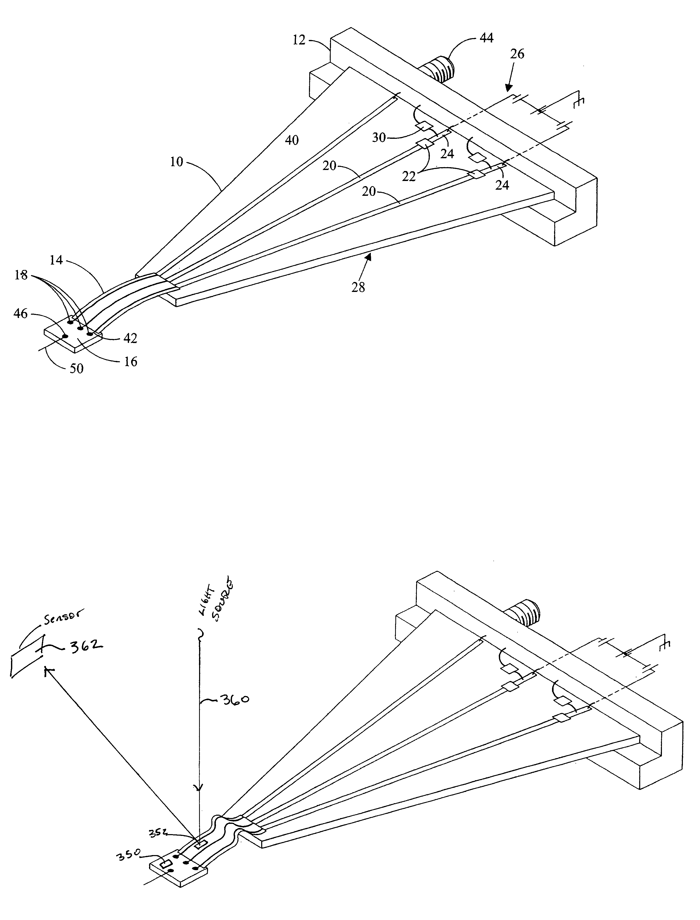
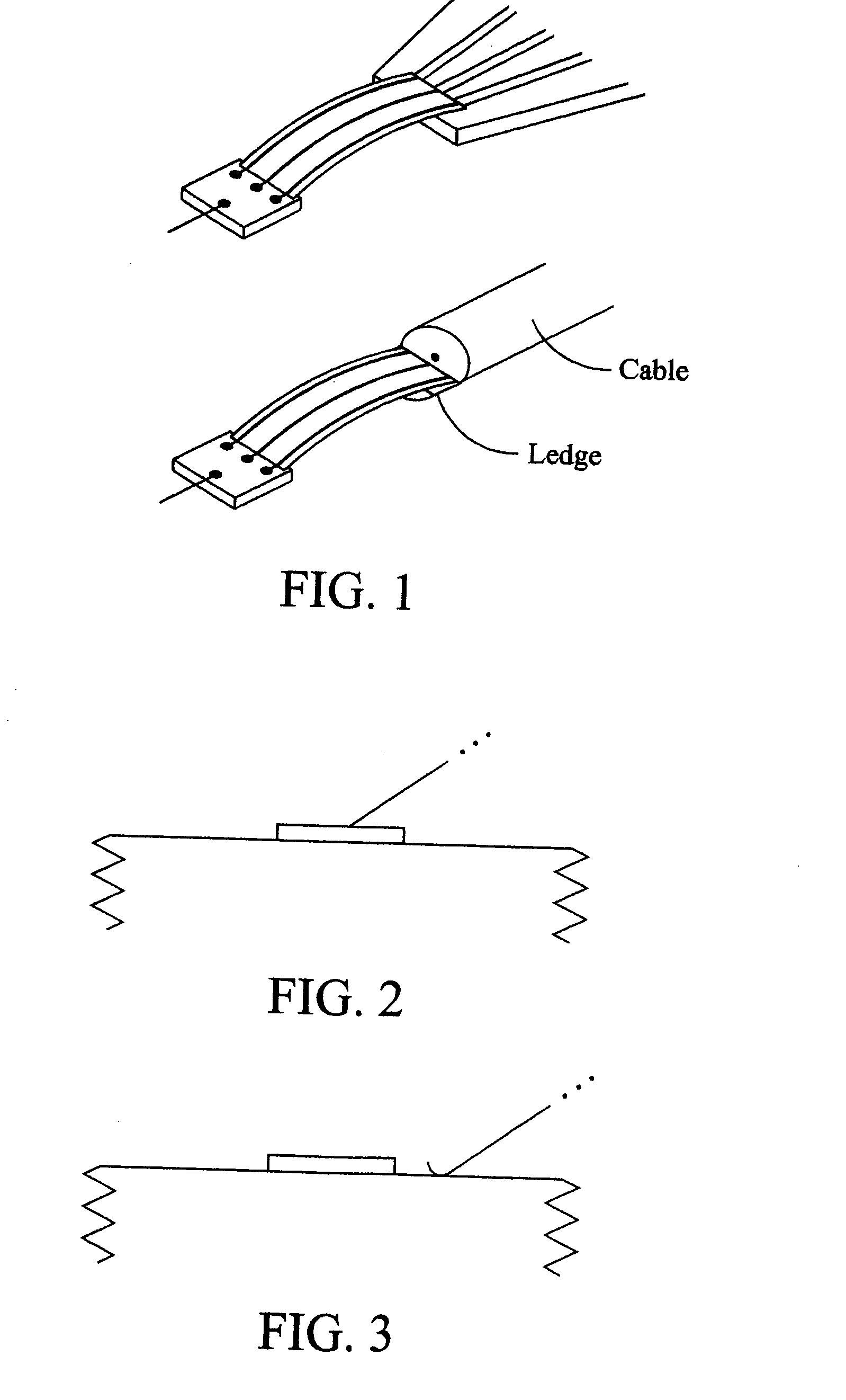
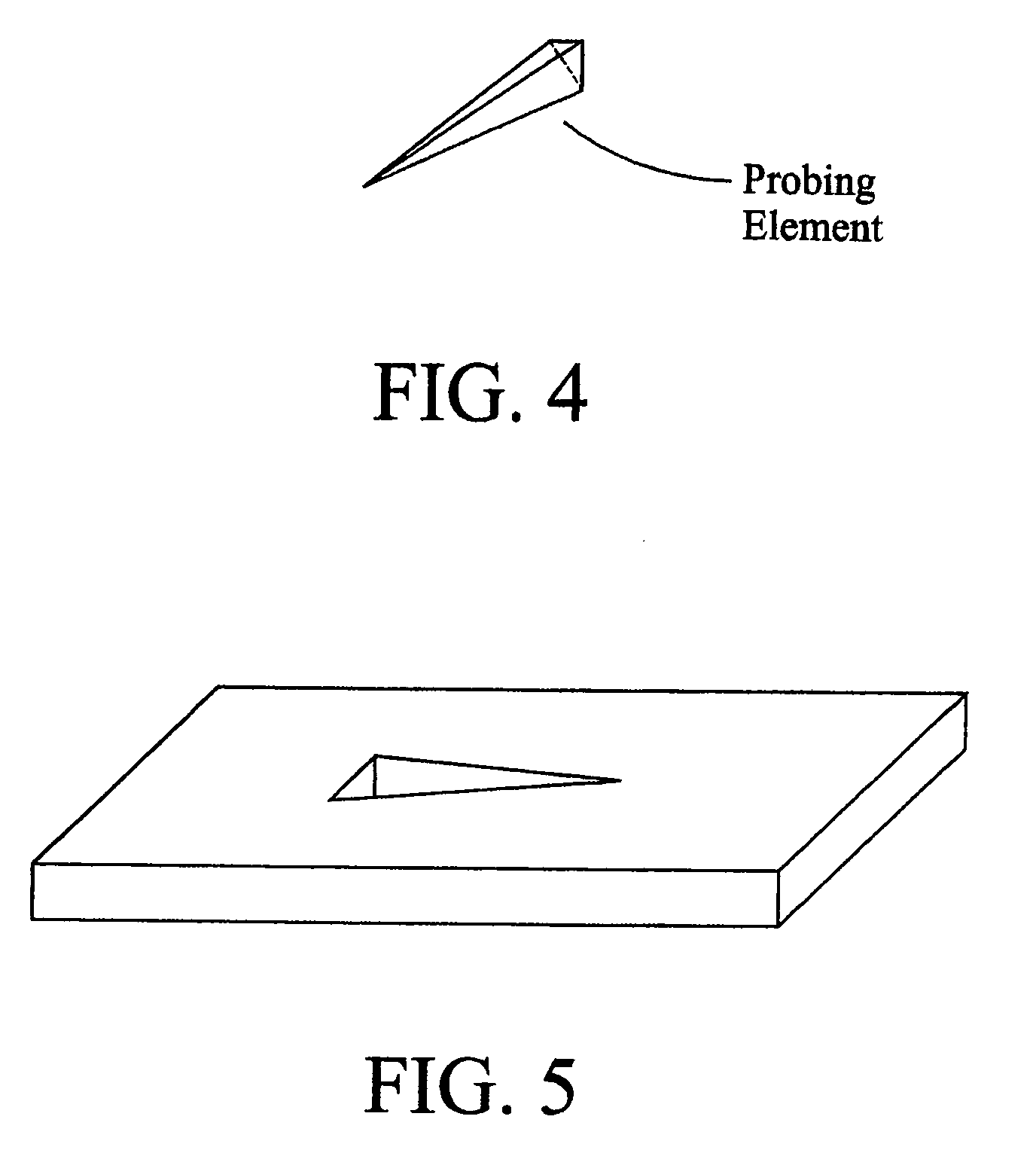
[0030] Active element based probes, such as those which include a high input resistance and / or low input capacitance amplifier circuit, tend to be suitable for probing circuitry where the addition of a capacitance on the order of approximately 100 fF for devices that are exceptionally small does not present a significant load to the circuitry. Most amplifier circuits include external power using a bias circuit, while passive circuitry may potentially be used. However, in some circumstances the loading of a circuit with 100 fF is simply unacceptable for effective measurements. For example, in some cases an opening is machined on the back side of a wafer that includes circuitry thereon to permit access to a conductive trace interconnecting a pair of transistor elements together, such as a pair of gates. With the continual shrinking of the size of the gate of transistors, together with the decrease in the amount of current used for switching the transistors, the loading of the circuit ...


PUM


Abstract

A probe suitable for probing a semiconductor wafer that includes an active circuit. The probe may include a flexible interconnection between the active circuit and a support structure. The probe may impose a relatively low capacitance on the device under test.

Description

CROSS-REFERENCE TO RELATED APPLICATIONS [0001] This application claims the benefit of U.S. Patent Application Ser. No. 60 / 532,756, filed Dec. 24, 2003, and U.S. Patent Application Ser. No. 60 / 589,346, filed Jul. 20, 2004.BACKGROUND OF THE INVENTION [0002] A probe suitable for probing a semiconductor wafer that includes an active circuit. BRIEF SUMMARY OF THE INVENTION [0003] There are many types of probing assemblies that have been developed for the measurement of integrated circuits and other forms of microelectronic devices. One representative type of assembly uses a circuit card on which the upper side is formed of elongate conductive traces that serve as signal and ground lines. A central opening is formed in the card, and a needle-like probe tip is attached to the end of each signal trace adjacent the opening so that a radially extending array of downwardly converging needle-like tips is presented by the assembly for selective connection with the closely spaced pads of the micr...

Claims


Application Information

Patent Timeline
IPC IPC(8): G01R1/067G01R31/02
CPCG01R1/06772G01R1/06711G01R1/06766G01R1/067G01R31/2886H01L22/00
Inventor STRID, ERICGLEASON, K. REED
Owner FORMFACTOR BEAVERTON INC
Why Eureka
Try Eureka