Erasable optical coupler

a technology of optical couplers and optical couplers, applied in nanotechnology, ion implantation coatings, coatings, etc., can solve the problems of high failure rate, increased cost, and unnecessary processing of failed chips, and achieve the effect of reducing processing wastage and minimising signal loss in the pic during operation

Active Publication Date: 2021-12-28
UNIV OF SOUTHAMPTON
View PDF8 Cites 0 Cited by
  • Summary
  • Abstract
  • Description
  • Claims
  • Application Information

AI Technical Summary

Benefits of technology

[0030]An erasable optical coupler as described above can be fabricated in a spatially efficient manner, preserving real estate on a photonic integrated chip (PIC). Furthermore, the erasable nature of the optical coupler allows removal after a testing procedure, resulting in minimal signal loss in the PIC during operation. Thus, the erasable optical coupler as described above enables the identification of defective chips during the fabrication process, reducing the processing wastage associated with PIC fabrication.

Problems solved by technology

This leads to high failure rates and unnecessary processing of failed chips, raising costs and lowering yield.
This limits the cost-effectiveness of PICs and their manufacture and therefore limits their uptake.
This testing at intermediate points allows the performance of individual photonic components or groups of components to be evaluated, hence allowing poor device performance or photonic circuit failures to be detected at an early stage.
Such a directional coupler is permanently fabricated within the photonic circuit, and cannot be removed after testing.
Therefore, the optical power that transfers through the directional coupler for testing is a permanent loss mechanism for the photonic circuit during normal operation.
As a result, a limited number of such structures can be used in a circuit, and the optical power available for testing at the directional coupler is limited.
Further, the optical power of the operational outputs of the photonic integrated circuit is similarly limited by the directional couplers provided for testing.

Method used


Image

  • Erasable optical coupler
  • Erasable optical coupler
  • Erasable optical coupler

Examples


Embodiment Construction

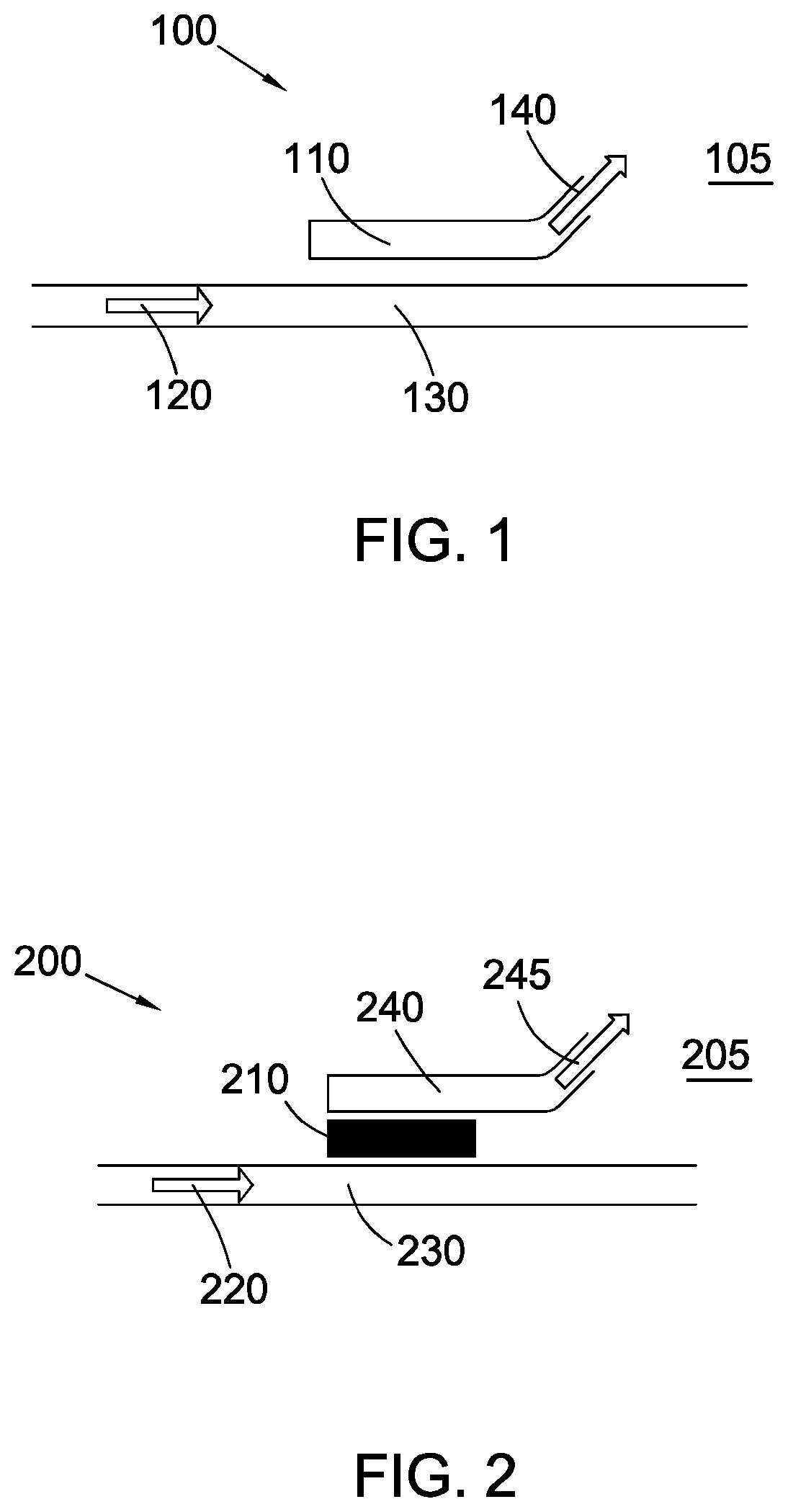
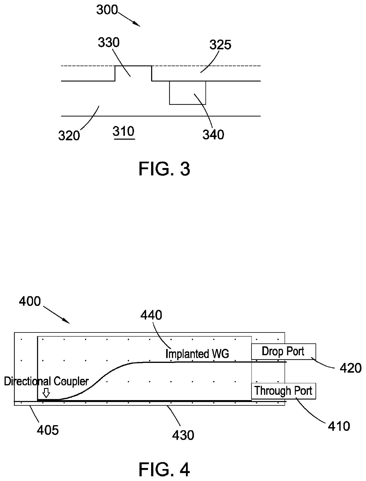
[0053]In the examples of the present disclosure, space-efficient erasable optical couplers for wafer-scale testing allow increased wafer real estate for photonic circuit fabrication. The optical couplers disclosed herein are directional couplers, and operate to couple operational and / or test wavelengths of light into or out of a conventional waveguide in a photonic circuit, for example provided as a PIC on an SOI wafer. FIGS. 1 and 2 show, in detail, such example photonic circuits 100, 200 including couplers.

[0054]An ion-implanted region in a PIC wafer material generally has a higher refractive index than the bulk material of that wafer 105, 205, and thus the examples of the present disclosure utilize this phenomenon to create an ion implanted region 110, 210 that forms an implanted waveguide optical coupler 110, 210 to couple light into and / or out of a conventional waveguide. With this ion implanted waveguide region 110, 210 formed adjacent to a conventional waveguide 130, 230, a d...


PUM

PropertyMeasurementUnit
implant energyaaaaaaaaaa
distanceaaaaaaaaaa
thickaaaaaaaaaa

Abstract

The disclosure provides a method of forming an erasable optical coupler in a photonic device comprising a conventional optical waveguide formed in a crystalline wafer. The method comprises selectively implanting ions in a localized region of the wafer material adjacent to the conventional waveguide of the photonic device, to cause modification of the crystal lattice structure of, and a change in refractive index in, the ion implanted region of the wafer material to thereby form an ion implanted waveguide optically coupled to the adjacent conventional waveguide to couple light out therefrom, or in thereto. The crystalline wafer material and ion implanted waveguide are such that the crystal lattice structure or composition can be modified to adjust or remove the optical coupling with the conventional waveguide by further modification of the refractive index in the ion implanted region.

Description

CROSS-REFERENCES TO RELATED APPLICATIONS[0001]This application claims priority to and is a continuation of International Patent Application No. PCT / GB2018 / 050651, filed Mar. 14, 2018; which claims priority from GB Patent Application No. 1704690.5, filed Mar. 24, 2017, the entire contents of which are hereby incorporated by reference in their entirety for all purposes.BACKGROUND OF THE INVENTION[0002]Generally photonic integrated chips (PICs) can only be tested at their inputs and outputs once fabrication is complete. This leads to high failure rates and unnecessary processing of failed chips, raising costs and lowering yield. This limits the cost-effectiveness of PICs and their manufacture and therefore limits their uptake. It would be desirable to improve the yield and cost effectiveness of PIC manufacture, and one way to do this is to facilitate improved wafer-scale testing throughout the manufacturing process.[0003]Wafer-scale autonomous testing is a crucial component of any larg...

Claims


Application Information

Patent Timeline
Patent Type & Authority Patents(United States)
IPC IPC(8): G02B6/34G02B6/134C23C14/48G01M11/00G02B6/12
CPCG02B6/1347C23C14/48G01M11/35G02B2006/12061G02B2006/12097G02B2006/12147G02B2006/12169G02B6/125B82Y20/00G02B6/12004G02B6/1225
Inventor CHEN, XIAMILOSEVIC, MILANREED, GRAHAM TREVORTHOMSON, DAVID JOHN
Owner UNIV OF SOUTHAMPTON
Why Eureka
Try Eureka