Sensor device

a sensor and sensor technology, applied in the field of sensor devices, can solve the problems of limited efficiency of the sensor, high undesirable noise components, and limited miniaturisation of such systems, and achieve the effects of improving the signal-to-noise ratio of the detection signal, increasing the amount of reflected light, and improving the angular resolution of the sensor devi

Active Publication Date: 2022-03-29
MELEXIS TECH NV
View PDF17 Cites 0 Cited by
  • Summary
  • Abstract
  • Description
  • Claims
  • Application Information

AI Technical Summary

Benefits of technology

[0010]The predetermined distance may be selected so as to minimise shadowing of the detection region by the emitter device.
[0013]The device may further comprise: an electrical coupling to the emitter device for providing power; the electrical coupling may be arranged to provide a thermal load, thereby reducing, when in use, thermal resistance between the emitter device and an environment in which the emitter device is disposed.
[0030]It is thus possible to provide a sensor device employing shared optics. The use of shared optics by the detector devices and the emitter devices enables larger optical components to be employed, thereby supporting an improved signal-to-noise ratio of a detection signal. In this regard, the sensor device permits an increased amount of reflected light to be received by the detector devices of the sensor device. Angular resolution of the sensor device is also improved. The sensor device also does not require complex control electronics to control the emitter device(s) and required beam collimation can be achieved. Furthermore, the sensor device is economic to manufacture. Additionally, owing to, for example, the spacing between the emitter device and the detector device and the effect of lens focusing, the sensor device no longer requires the emitter surface of the emitter device to be smaller in surface area than the detector surface of the detector device.

Problems solved by technology

Such an illumination technique requires the use of large and dedicated projection optics to achieve adequate beam shaping, which limits miniaturisation of such systems and so integration into, for example, mass-produced commercial vehicles.
Furthermore, due to mechanical constraints, the device that emits the laser light needs to be physically separated far enough from the device that detects the reflected light.
However, due to the generally reciprocal nature of the design of such optics, a reflected signal from the reflecting target is primarily focused back onto the emitter and not onto the detector.
By intentionally de-focusing the lens or by virtue of the imperfect nature of the lens assembly, a part of the reflected light can be incident on the detector, but the amount of reflected light incident upon the detector is only a small proportion of the overall light reflected by the reflecting target and so the efficiency of the sensor is described in U.S. Pat. No. 4,460,259 is limited.
Also, integrating a highly sensitive detector and a powerful emitter or emitter driver on the same semiconductor substrate poses significant challenges in terms of electrical, optical and thermal noise coupling, such noise components being highly undesirable.
Therefore, the integration approach described is not viable for sensor implementations employing a large number of elements as described above.
The physical distance between the emitter lens and the receiving lens also gives rise to parallax errors, which limits the operating distance range of known sensors, especially at close range.
To mitigate this problem, it is known to employ projecting optics, rotating mechanical mirrors or microelectromechanical systems (MEMS) mirrors can be used to scan a laser spot across a scene, but such systems require very complex electronics to control the angle of the laser beam.
However, such an approach does not satisfy a sufficient beam collimation requirement of time-of-flight illumination systems relying on structured light pattern projection due to the limited size of each miniature lens.

Method used


Image

  • Sensor device
  • Sensor device
  • Sensor device

Examples


Embodiment Construction

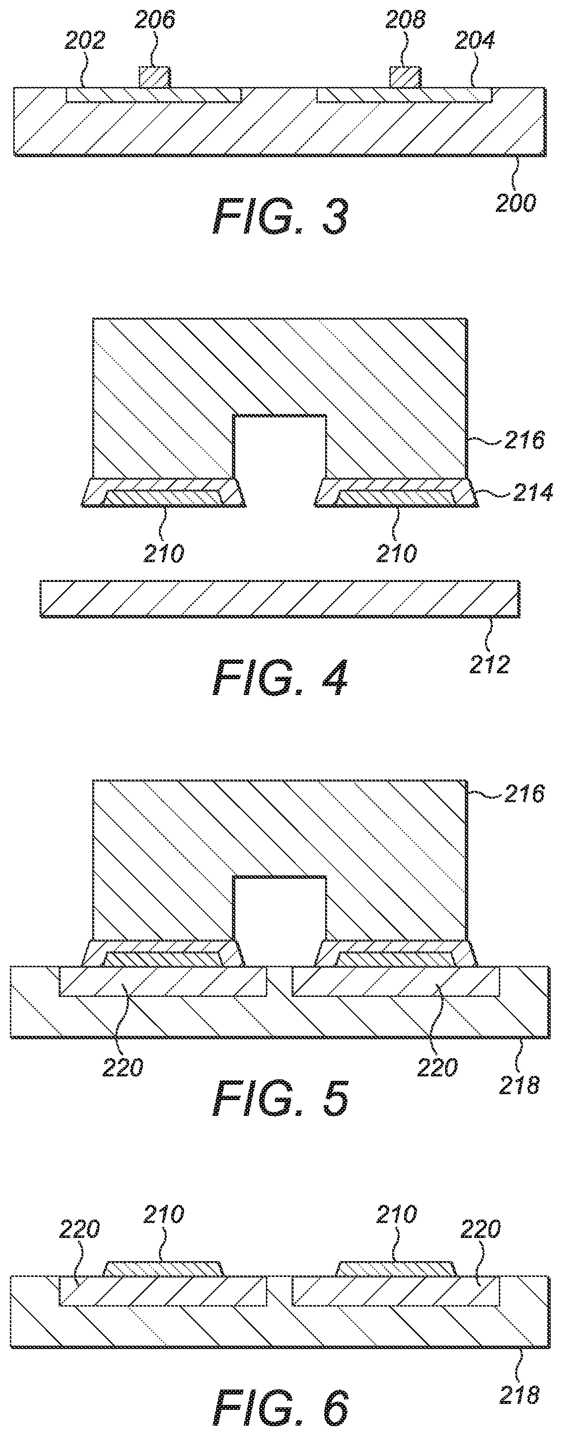
[0039]Throughout the following description identical reference numerals will be used to identify like parts.

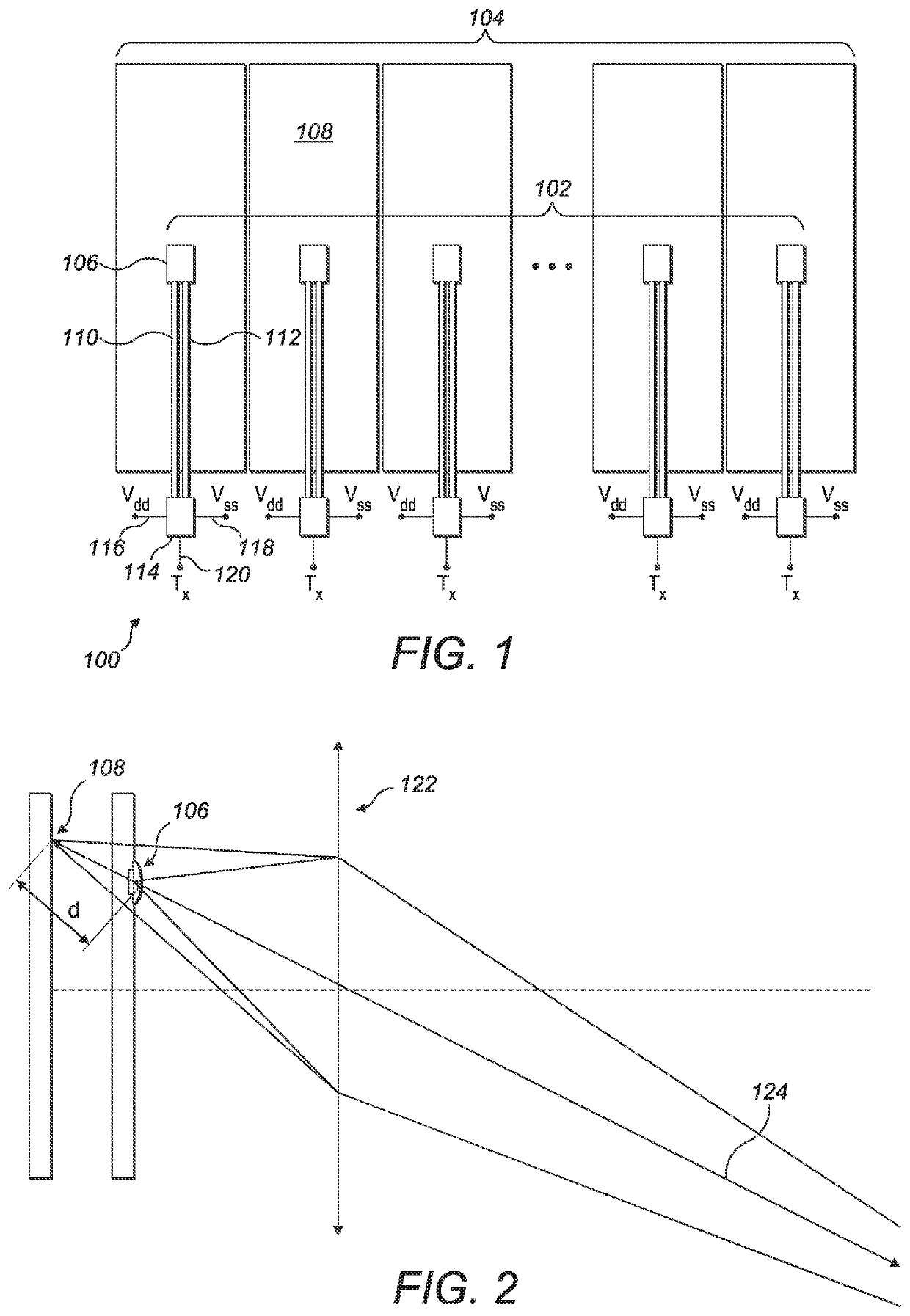
[0040]Time-of-flight measurement systems and other systems, for example night vision system, comprise one of more sensor devices, for example optical sensor devices. Referring to FIG. 1, a sensor device 100 comprises, in this example, a plurality of emitter devices 102 for emitting electromagnetic radiation, for example light, for example an array of emitter devices, and a plurality of detector devices 104 for detecting electromagnetic radiation, for example light, for example an array of detector devices. The plurality of emitter devices 102 respectively have an emitter region from which the light is emitted, and the plurality of emitter devices 102 respectively reside on a first surface. The plurality of detector devices 104 respectively have a detector region through which light to be detected propagates, and the plurality of detector devices 104 respectively reside in a se...


PUM


Abstract

A sensor device (100) comprises an emitter device (106) arranged to emit electromagnetic radiation and having an emission region associated therewith. The sensor device (100) also comprises a detector device (108) arranged to receive electromagnetic radiation and having a detection region associated therewith, and an optical system (122). The emission region is spaced at a predetermined distance from the detection region. The optical system (122) defines a plurality of principal rays, a number of the plurality of principal rays intersecting the detection region. The number of the plurality of principal rays also intersect the emission region.

Description

FIELD OF THE INVENTION[0001]The present invention relates to a sensor device of the type that, for example, comprises an emitter device for emitting electromagnetic radiation and a detector device for receiving a portion of the electromagnetic radiation reflected by a target.BACKGROUND OF THE INVENTION[0002]In so-called time-of-flight sensing systems and other systems, for example night vision systems, it is known to employ an illumination source to illuminate a surrounding environment within a field of view of the illumination source, sometimes known as a “scene”. International patent publication no. WO 2017 / 068199 describes an approach that relies on the projection of discrete spots of laser light onto a scene of interest. Such an illumination technique requires the use of large and dedicated projection optics to achieve adequate beam shaping, which limits miniaturisation of such systems and so integration into, for example, mass-produced commercial vehicles. Also, it is desirable...

Claims


Application Information

Patent Timeline
Patent Type & Authority Patents(United States)
IPC IPC(8): G01S7/481G01S17/02H01L31/12H01L27/146G01S17/04G01S17/894
CPCG01S7/4813G01S7/4812G01S17/04H01L27/146H01L31/12G01S7/4811G01S17/894
Inventor KOERS, GAETANLETEN, WOUTERMADDALENA, SAMKAY, ROSS
Owner MELEXIS TECH NV
Why Eureka
Try Eureka