Check patentability & draft patents in minutes with Patsnap Eureka AI!

Enhanced substrate amorphization using intermittent ion exposure

a technology of ion exposure and enhanced substrate, applied in the field of semiconductor substrate processing, can solve the problems of significant sputtering and swelling of the substrate, modification of the composition of the substrate, and formation of damage accumulation,

Active Publication Date: 2022-04-26
APPLIED MATERIALS INC
View PDF9 Cites 0 Cited by
  • Summary
  • Abstract
  • Description
  • Claims
  • Application Information

AI Technical Summary

Benefits of technology

This approach enables precise control over the degree of amorphization and damage accumulation, reducing the total ion dose required for amorphization, minimizing substrate damage, and increasing productivity by allowing amorphization at room temperature with lower sputtering and swelling, and providing precise control over the PAI process.

Problems solved by technology

Damage accumulation may be formed at approximately the depth of the maximum nuclear energy loss.
Side effects of the high dose implantation include significant sputtering and swelling of the substrate and modification of substrate composition.
In some cases, forming an amorphous oxide layer over the substrate may be used to reduce the channeling effects in the PAI implant species, while resulting in additional process steps for formation of the oxide layer and possible contamination of oxygen from the oxide layer into the underlying matrix due to ion beam mixing.

Method used


Image

  • Enhanced substrate amorphization using intermittent ion exposure
  • Enhanced substrate amorphization using intermittent ion exposure
  • Enhanced substrate amorphization using intermittent ion exposure

Examples


Embodiment Construction

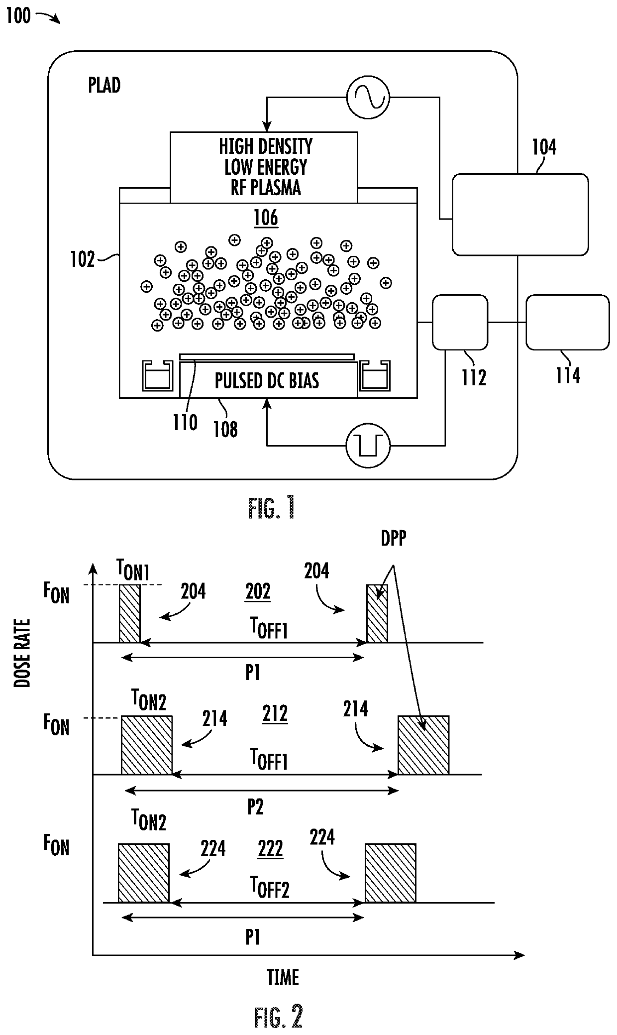
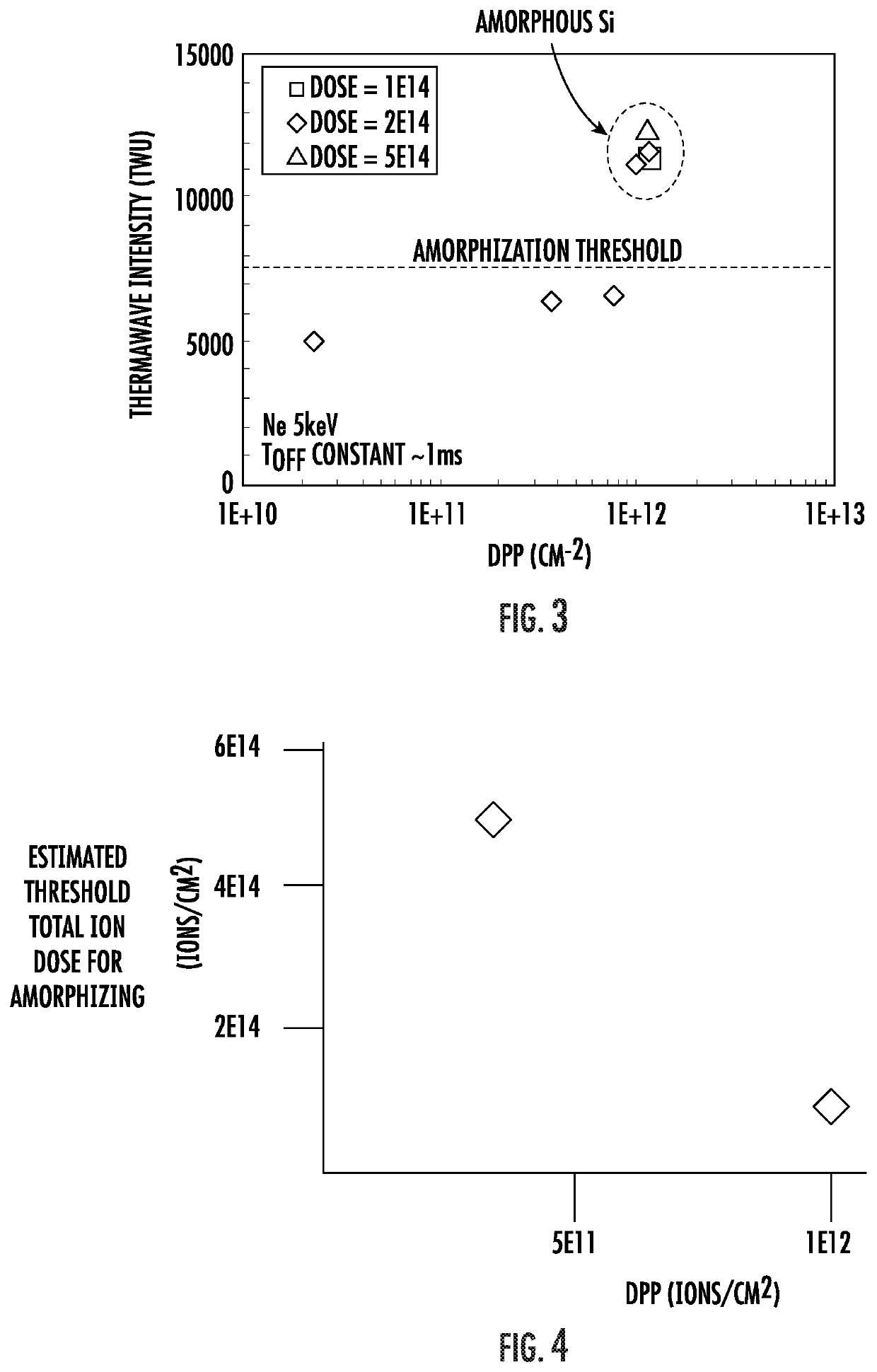
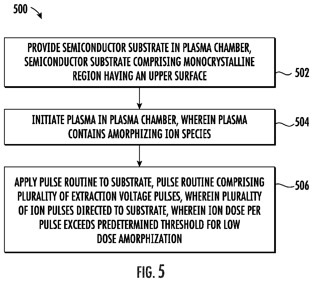
[0015]The present embodiments will now be described more fully hereinafter with reference to the accompanying drawings, in which exemplary embodiments are shown. The embodiments are not to be construed as limited to the embodiments set forth herein. Rather, these embodiments are provided so that this disclosure will be thorough and complete, and will fully convey their scope to those skilled in the art. In the drawings, like numbers refer to like elements throughout.

[0016]In the following description and / or claims, the terms “on,”“overlying,”“disposed on” and “over” may be used in the following description and claims. “On,”“overlying,”“disposed on” and “over” may be used to indicate that two or more elements are in direct physical contact with one another. Also, the term “on,”, “overlying,”“disposed on,” and “over”, may mean that two or more elements are not in direct contact with one another. For example, “over” may mean that one element is above another element while not contactin...


PUM

PropertyMeasurementUnit
TON timeaaaaaaaaaa
voltageaaaaaaaaaa
thresholdaaaaaaaaaa

Abstract

A method may include providing a substrate in a plasma chamber, the substrate comprising a monocrystalline semiconductor, having an upper surface. The method may include initiating a plasma in the plasma chamber, the plasma comprising an amorphizing ion species, and applying a pulse routine to the substrate, the pulse routine comprising a plurality of extraction voltage pulses, wherein a plurality of ion pulses are directed to the substrate, and wherein an ion dose per pulse is greater than a threshold for low dose amorphization.

Description

BACKGROUNDField[0001]Embodiments relate to the field of semiconductor processing, an in particular, to pulsed plasma processing apparatus and techniques for processing semiconductor substrates.Discussion of Related Art[0002]Pre-amorphization implant (PAI) is a well-established technique that has frequently been used in semiconductor device fabrication processes. The PAI process employs energetic ions to completely disrupt crystal lattice structure of a crystalline substrate through inelastic electronic or nuclear collisions. Damage accumulation may be formed at approximately the depth of the maximum nuclear energy loss. Increasing ion dose may result in a formation of amorphous region and extension of the amorphous region toward the given substrate surface.[0003]Notably, PAI is often used in conjunction with an additional ion implantation process, in order to better control the placement of ions within a substrate during the additional ion implantation process. For example, a PAI im...

Claims


Application Information

Patent Timeline
Patent Type & Authority Patents(United States)
IPC IPC(8): H01L21/223H01L21/265H01L21/02H01J37/317
CPCH01L21/2236H01J37/3171H01L21/02658H01L21/265H01L21/28518H01J37/32357H01J37/32422H01J37/32706
Inventor CHARNVANICHBORIKARN, SUPAKITHATEM, CHRISTOPHER R.
Owner APPLIED MATERIALS INC
Features
  • R&D
  • Intellectual Property
  • Life Sciences
  • Materials
  • Tech Scout
  • Unparalleled Data Quality
  • Higher Quality Content
  • 60% Fewer Hallucinations
Learn More