
Light-emitting element having commonly formed hole transport layer and anode electrode and light-emitting device

a technology of light-emitting elements and transport layers, which is applied in the direction of solid-state devices, electric lighting sources, electric lighting sources, etc., can solve the problems of reducing the efficiency of recombination in a light-emitting layer between positive holes from an anode electrode and electrons from a cathode electrode, complicated structure of light-emitting elements, and increasing the cost of production. , to achieve the effect of maintaining the transport efficiency of positive holes

Active Publication Date: 2022-05-24
SHARP KK
View PDF39 Cites 0 Cited by
  • Summary
  • Abstract
  • Description
  • Claims
  • Application Information

AI Technical Summary

Benefits of technology

The invention described in this patent text simplifies the structure of a light-emitting element while maintaining the efficiency of transporting positive holes and electrons from electrodes to the light-emitting layer. It also helps to maintain the luminous efficiency of the element.

Problems solved by technology

When a hole transport layer and an electron transport layer are formed in each subpixel, there is a problem in that a structure of a light-emitting element becomes complicated, and a manufacturing step of the light-emitting element also becomes complicated and takes quite some time.
However, when the hole transport layer and the electron transport layer are formed in common to all of the subpixels, there is a problem in that efficiency of recombination in a light-emitting layer between positive holes from an anode electrode and electrons from a cathode electrode decreases depending on a type of the subpixels.

Method used


Image

  • Light-emitting element having commonly formed hole transport layer and anode electrode and light-emitting device
  • Light-emitting element having commonly formed hole transport layer and anode electrode and light-emitting device
  • Light-emitting element having commonly formed hole transport layer and anode electrode and light-emitting device

Examples


first embodiment

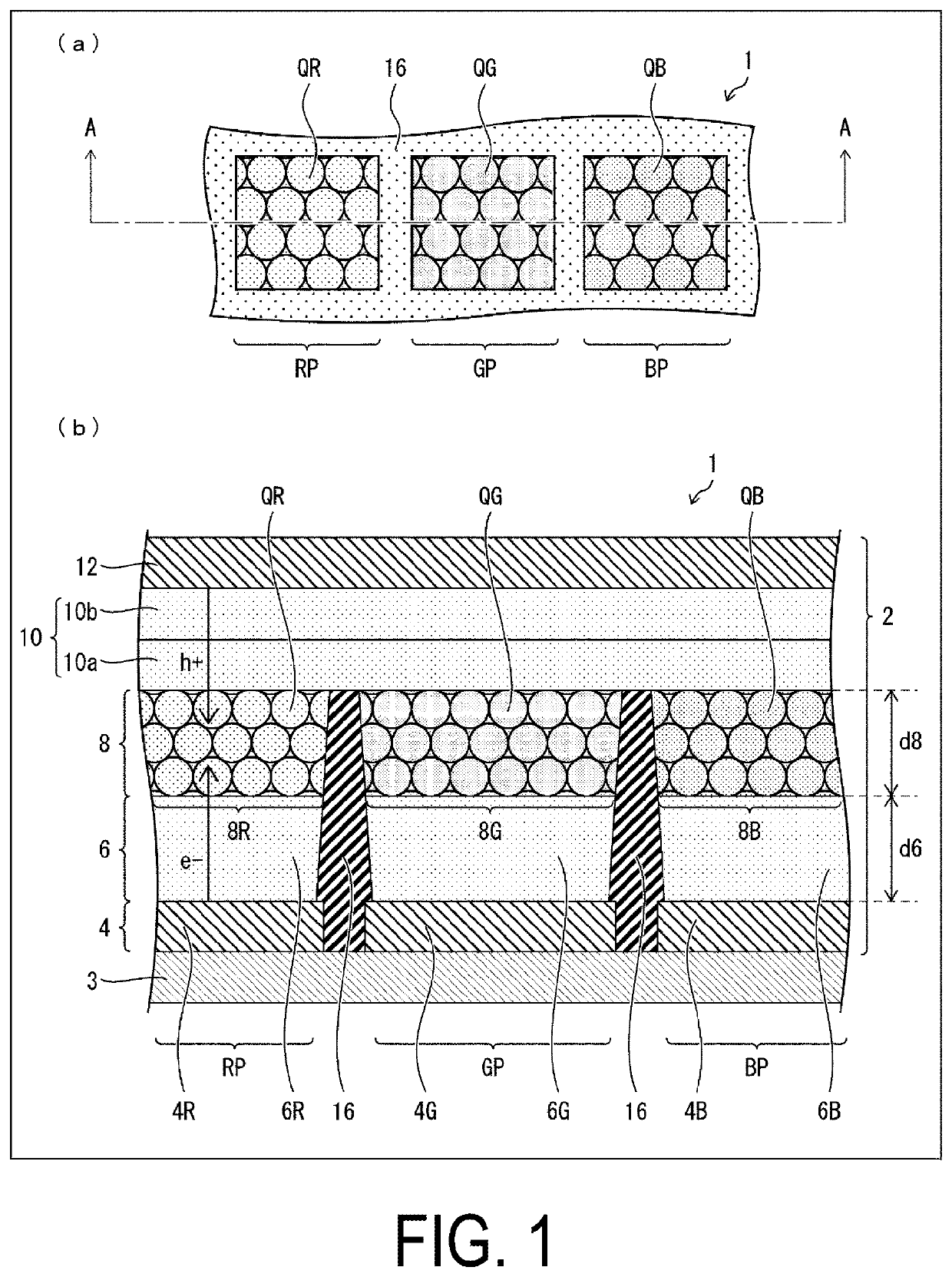
[0019](a) of FIG. 1 is a schematic top view of a light-emitting device 1 according to the present embodiment. (b) of FIG. 1 is a cross-sectional view taken along a line A-A in the direction of the arrows in (a) of FIG. 1. Note that, in (a) of FIG. 1, an upper face of the light-emitting device 1 is illustrated by transmitting through a hole transport layer 10 and an anode electrode 12 in order to make detailed illustrate a light-emitting layer 8 described below.

[0020]As illustrated in (b) of FIG. 1, the light-emitting device 1 according to the present embodiment includes a light-emitting element 2 and an array substrate 3. The light-emitting device 1 has a structure in which respective layers of the light-emitting element 2 are layered on the array substrate 3 in which a thin film transistor (TFT; not illustrated) is formed. In the present specification, a direction from the light-emitting element 2 to the array substrate 3 of the light-emitting device 1 is referred to as “downward,”...

second embodiment

[0077]FIG. 5 is a schematic diagram illustrating a light-emitting device 1 according to the present embodiment. (a) and (b) of FIG. 5 correspond to (a) and (b) of FIG. 1, respectively.

[0078]A light-emitting element 2 in the present embodiment is different from the light-emitting element 2 in the previous embodiment in that a blue pixel electron transport layer 6B includes a first blue pixel electron transport layer 6Ba and a second blue pixel electron transport layer 6Bb. The first blue pixel electron transport layer 6Ba and the second blue pixel electron transport layer 6Bb each include a different material, and the second blue pixel electron transport layer 6Bb is formed on an upper layer of the first blue pixel electron transport layer 6Ba.

[0079]The light-emitting element 2 in the present embodiment is also different from the light-emitting element 2 in the previous embodiment in that a red pixel electron transport layer 6R, a green pixel electron transport layer 6G, and the blue...

third embodiment

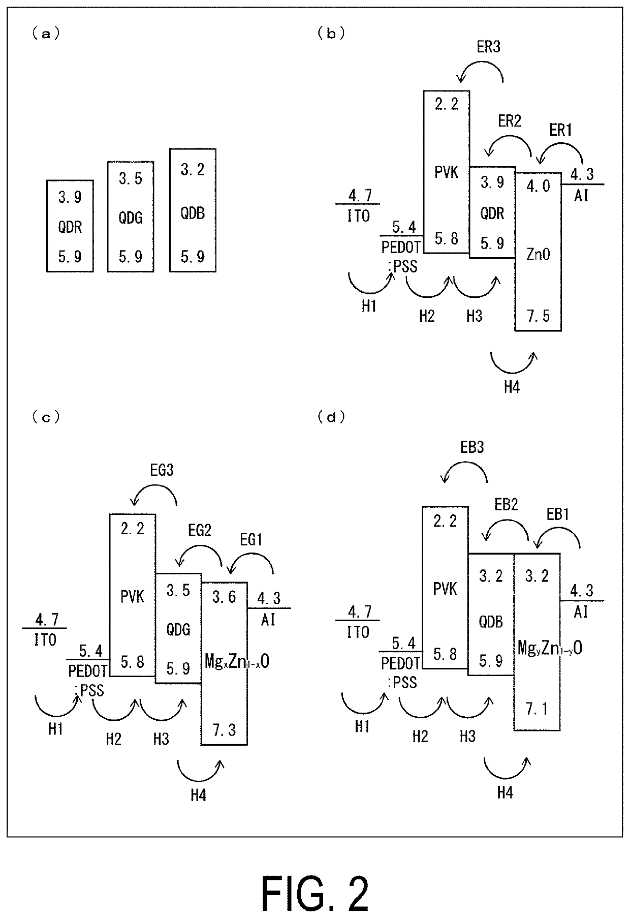
[0091]FIG. 8 is an energy diagram illustrating an example of a Fermi level, an electron affinity, and an ionization potential in each layer of a blue subpixel BP of a light-emitting element 2 according to the present embodiment. FIG. 8 illustrates an energy diagram of a blue pixel cathode electrode 4B, a blue pixel electron transport layer 6B, a blue pixel light-emitting layer 8B, a first hole transport layer 10a, a second hole transport layer 10b, and an anode electrode 12 from the right to the left.

[0092]The light-emitting device 1 according to the present embodiment may have the same configuration as that of the light-emitting device 1 illustrated in FIG. 1 except that a material included in the blue pixel electron transport layer 6B is different. In the present embodiment, the blue pixel electron transport layer 6B includes MgzZn1-zO. Here, z indicates a percentage of Zn of ZnO replaced with Mg, and 0≤z≤1.

[0093]Here, in the present embodiment, the blue pixel electron transport l...


PUM

PropertyMeasurementUnit
wavelength bandaaaaaaaaaa

Abstract

For a purpose of simplifying a structure of a light-emitting element while maintaining luminous efficiency of the light-emitting element, the present invention provides a light-emitting element including: a cathode electrode; an anode electrode; a light-emitting layer between the cathode electrode and the anode electrode; an electron transport layer between the light-emitting layer and the cathode electrode; and a hole transport layer between the light-emitting layer and the anode electrode. The light-emitting element further includes a plurality of subpixels for each light emission wavelength of the light-emitting layer, the light-emitting layer and the electron transport layer for each of the plurality of subpixels, and the hole transport layer common to at least the plurality of subpixels.

Description

TECHNICAL FIELD[0001]The disclosure relates to a light-emitting element including quantum dots, a light-emitting device including the light-emitting element, a manufacturing method of a light-emitting element, and a manufacturing apparatus of a light-emitting element.BACKGROUND ART[0002]PTL 1 discloses an organic electroluminescence image device including a plurality of pixels. In JP 2010-244885 A (published on Oct. 28, 2010), each of the pixels includes a light-emitting element including an anode electrode, a hole transport layer, a light-emitting layer, an electron transport layer, and a cathode electrode. Furthermore, JP 2010-244885 A (published on Oct. 28, 2010) 1 describes a configuration in which a different light-emitting layer is formed for each subpixel, and a hole transport layer and an electron transport layer are similarly formed for each subpixel.SUMMARY[0003]When a hole transport layer and an electron transport layer are formed in each subpixel, there is a problem in t...

Claims


Application Information

Patent Timeline
Patent Type & Authority Patents(United States)
IPC IPC(8): H01L29/08H01L51/50H01L27/32H01L51/56
CPCH01L51/5056H01L27/3244H01L51/502H01L51/5072H01L51/56H01L2227/323H05B33/10H05B33/12H05B33/14H05B33/02H10K59/38H10K50/115H10K50/16H10K2102/00H10K59/12H10K50/15H10K71/00H10K59/1201
Inventor SAKAKIBARA, YUSUKEKIMOTO, KENJIRYOHWA, TATSUYA
Owner SHARP KK
Learn More