Microwave antenna apparatus

a technology of antenna apparatus and microwave, applied in the direction of cross-talk/noise/interference reduction, instruments, and semiconductor/solid-state device details, etc., can solve the problems of distorted radiation pattern, high amount of parasitic radiation to all directions, and narrow bandwidth (1-5%)

Active Publication Date: 2022-05-31
SONY CORP
View PDF16 Cites 1 Cited by
  • Summary
  • Abstract
  • Description
  • Claims
  • Application Information

AI Technical Summary

Benefits of technology

[0009]It is an object to provide a microwave antenna apparatus that couples the RF signal from RDL layer to the antenna on eWLB and that reduces unwanted ripples and surface waves.
[0013]One of the aspects of the disclosure is to overcome unwanted ripples in the radiation pattern and surface waves, by providing electromagnetic band gap structures (EBGs) (the EBG module) that may be integrated on a PCB layer used as carrier and couple the EBG module to the RDL layer of the package module, e.g. via solder balls. Signal and power interconnects that are required between the eWLB package and the PCB arrangement may be provided by not filling the complete surface of the PCB with EBGs which enables placement of coupling element like solder balls or pins with current manufacturing technology. The proposed solution thus presents a practical realization of EBGs having the same performance as an ideal EBG realized on an infinite plane.

Problems solved by technology

The disadvantage of the aforementioned solutions is their narrow bandwidth (1-5%), distorted radiation patterns, and the high amount of parasitic radiation to all directions.
One of the most important challenges for such package antennas is on one hand to couple the RF signal from RDL layer to the antenna on eWLB and on the other hand to reduce the ripples caused by epoxy and reflector placed on a PCB layer conventionally used a carrier.

Method used


Image

  • Microwave antenna apparatus
  • Microwave antenna apparatus
  • Microwave antenna apparatus

Examples


first embodiment

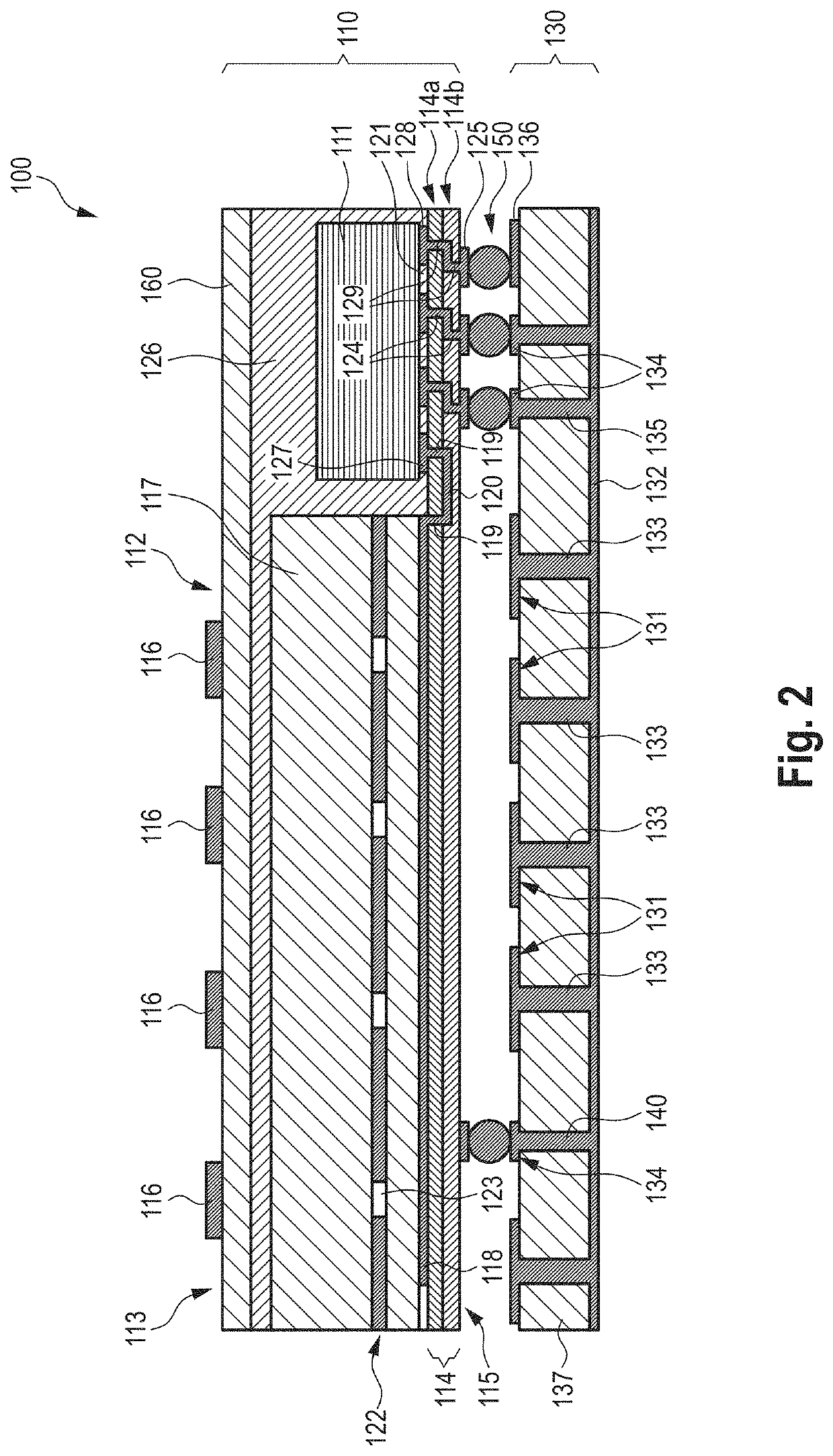
[0035]The present disclosure presents a solution for this problem by adding an electromagnetic band gap (EBG) structure below the package module as illustrated in FIG. 2 showing a microwave antenna apparatus 100 according to the present disclosure. The microwave antenna apparatus 100 generally comprises a package module 110 and an EBG module 130 coupled to the package module 110, in particular to a redistribution layer of the package module 110, via solder balls 150.

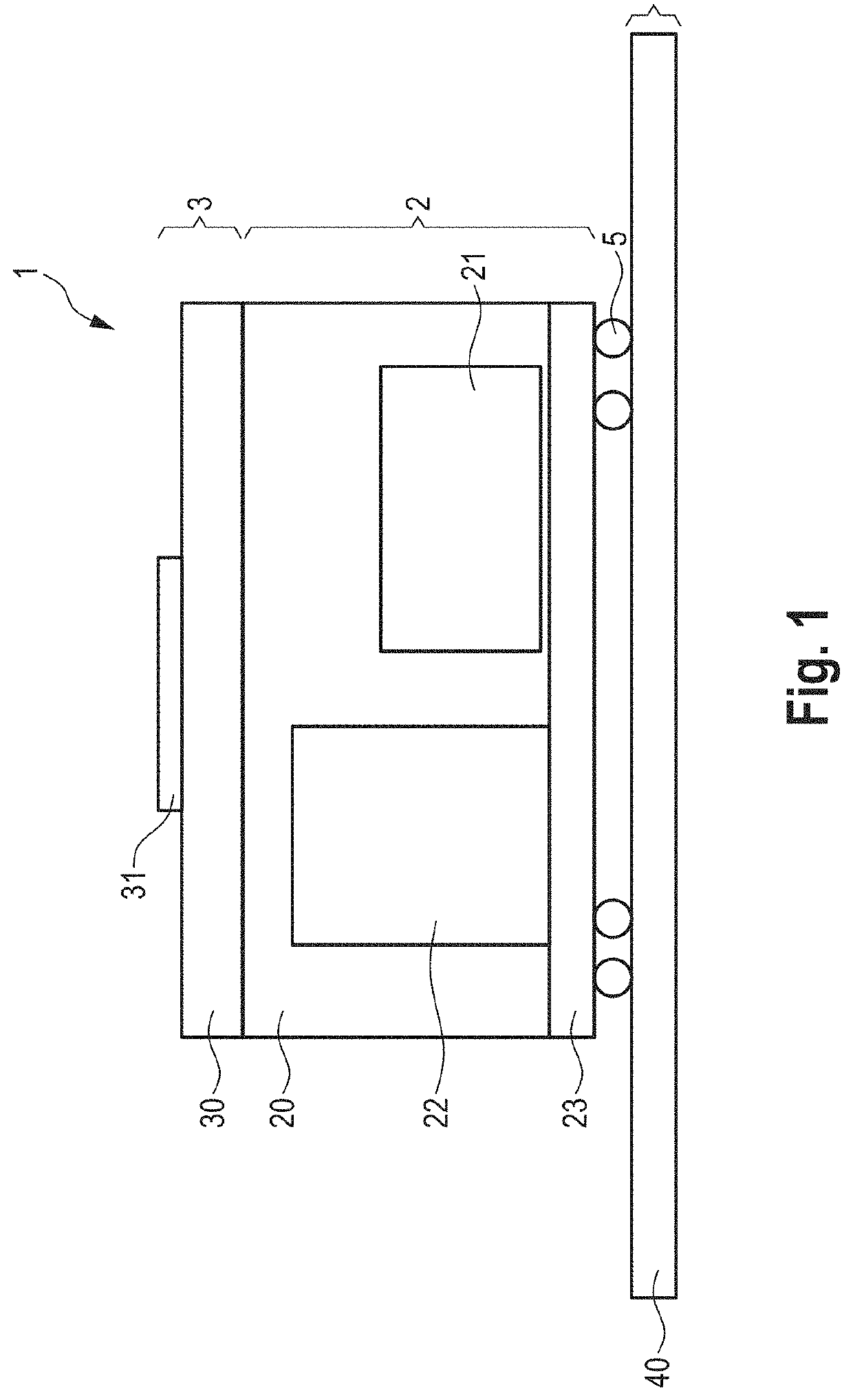
[0036]The package module 110 generally comprises a semiconductor unit 111 (also called chip), an antenna unit 112 arranged on a first side 113 of the package module 110 and a redistribution layer (RDL) unit 114 (in this embodiment comprising two redistribution layers 114a, 114b; in other embodiments comprising a redistribution layer) arranged on a second side 115 of the package module 110 opposite the first side 113. The semiconductor unit 111 is embedded in a mold layer 126. The antenna elements 116 are provided on top ...

second embodiment

[0046]FIG. 7 shows a microwave antenna apparatus 400 according to the present disclosure. As far as possible the same reference numeral are used as in FIG. 2 to reference the same elements.

[0047]The microwave antenna apparatus 400 comprises a semiconductor package module 410, an EBG module 430 coupled to the semiconductor package module 410 via solder balls 150 and a PoP antenna module 450 coupled to the semiconductor package module 410 via solder balls 151. A first RDL layer group 114a (comprising one or more polymer layer or RDL layers) is arranged on the bottom side of the semiconductor package module 410 and a second RDL layer group 114b is arranged on the top side of the semiconductor package module 410. Thus, in this embodiment separate RDL layer groups 114a, 114b are arranged on two sides of the semiconductor package module 410.

[0048]In this embodiment the RF signal is coupled from the chip 111 to the antenna elements 116 via the microstrip through the coupling element 117 as...

embodiment 3

[0081]4. Microwave antenna apparatus as defined in embodiment 3,

[0082]wherein the EBG area has at least the same size as the antenna area.

[0083]5. Microwave antenna apparatus as defined in embodiment 3 or 3,

[0084]wherein the EBG module comprises a ground layer arranged on the first surface of the EBG module around the EBG area.

[0085]6. Microwave antenna apparatus as defined in any one of embodiments 2 to 5,

[0086]wherein the one or more EBG cells are mushroom type EBG cells, uni-planar type EBG cells, polarization dependent EBG cells, compact spiral EBG cells, stacked EBG cells, miniaturized EBG cells, or interdigital capacitor EBG cells.

[0087]7. Microwave antenna apparatus as defined in any preceding embodiment,

[0088]wherein the EBG module comprises an EBG substrate layer, one or more EBG patches arranged on a first surface of the EBG substrate layer facing the package module, and one or more solder ball pads arranged on the first surface of the EBG substrate layer and contacting th...


PUM


Abstract

A microwave antenna apparatus comprises a package module comprising a semiconductor unit, an antenna unit arranged on a first side of the package module and a redistribution layer group arranged on a second side of the package module opposite the first side, and an electromagnetic band gap structure, EBG, module coupled to the redistribution layer group of the package module.

Description

CROSS-REFERENCE TO RELATED APPLICATION[0001]The present application claims priority to EP 19165279.1, filed Mar. 26, 2019, the entire contents of which are incorporated herein by reference.BACKGROUNDField of the Disclosure[0002]The present disclosure relates to a microwave antenna apparatus.Description of Related Art[0003]Fan-out wafer level packaging technology such as the embedded wafer-level ball grid array (eWLB) is a mature technology for mm-wave radar and communication systems. This packaging technology is the first choice for low-cost system integration of MMICs, passives, and antennas into a single plastic package.[0004]In academic research many different types of planar antenna structures have been published so far. They all have in common, that the antenna elements are printed on one or more redistribution layers (RDLs). The integration and interconnection between the chip and antenna is performed at RDL level.[0005]The disadvantage of the aforementioned solutions is their...

Claims


Application Information

Patent Timeline
Patent Type & Authority Patents(United States)
IPC IPC(8): H05K1/02H01Q15/00H01Q23/00H01L23/66H01L23/00G01S7/03
CPCH05K1/0236H01L23/66H01L24/13H01Q15/008H01Q23/00G01S7/032H01L2223/6677H01L2224/1623H01L2224/16227H01Q1/38H01Q21/065
Inventor KHAN, WASIF TANVEERWALEED, AHMADOTT, ARNDT THOMASHOTOPAN, RAMONA
Owner SONY CORP
Why Eureka
Try Eureka