Eureka AIR delivers breakthrough ideas for toughest innovation challenges, trusted by R&D personnel around the world.

Split gate (SG) memory device and novel methods of making the SG-memory device

Active Publication Date: 2022-09-20
GLOBALFOUNDRIES US INC
View PDF9 Cites 2 Cited by
  • Summary
  • Abstract
  • Description
  • Claims
  • Application Information

AI Technical Summary

Benefits of technology

The patent discloses new ways to make an SG-memory device, which is a type of memory integrated circuit. These methods involve using a conductive selection gate electrode and a conductive memory gate electrode that have specific shapes and positions relative to each other. The device also includes layers of insulating material that are positioned between the electrodes and the semiconductor substrate. The technical effects of these new methods may include improved performance and efficiency of the SG-memory device.

Problems solved by technology

This difference in height makes embedding such flash memory devices on a substrate with logic devices challenging.

Method used


Image

  • Split gate (SG) memory device and novel methods of making the SG-memory device
  • Split gate (SG) memory device and novel methods of making the SG-memory device
  • Split gate (SG) memory device and novel methods of making the SG-memory device

Examples


Embodiment Construction

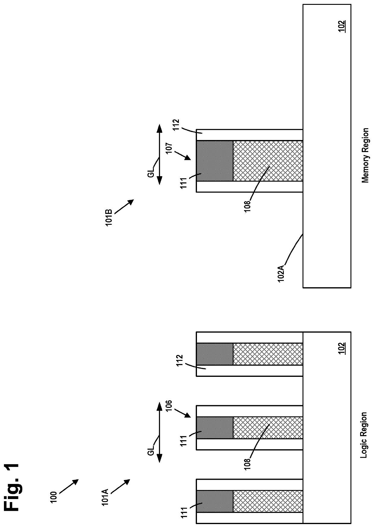
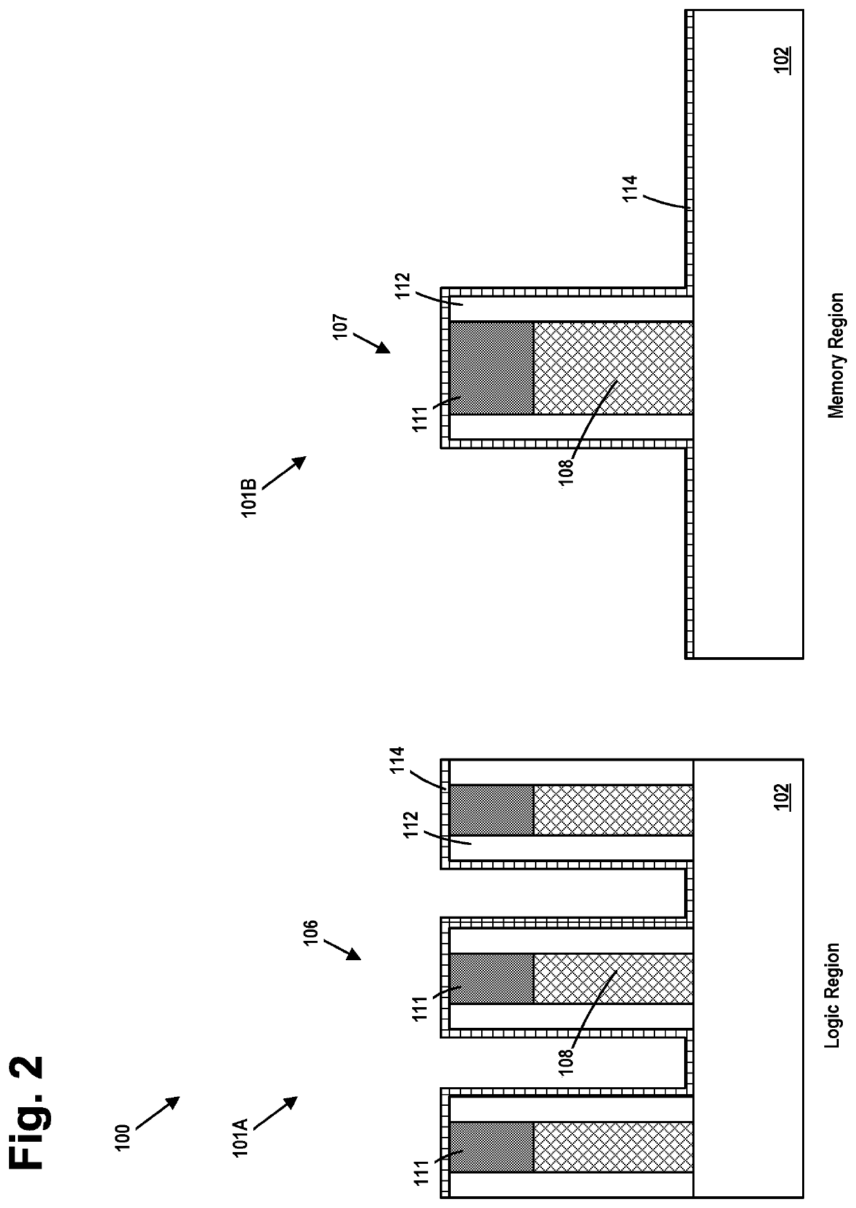
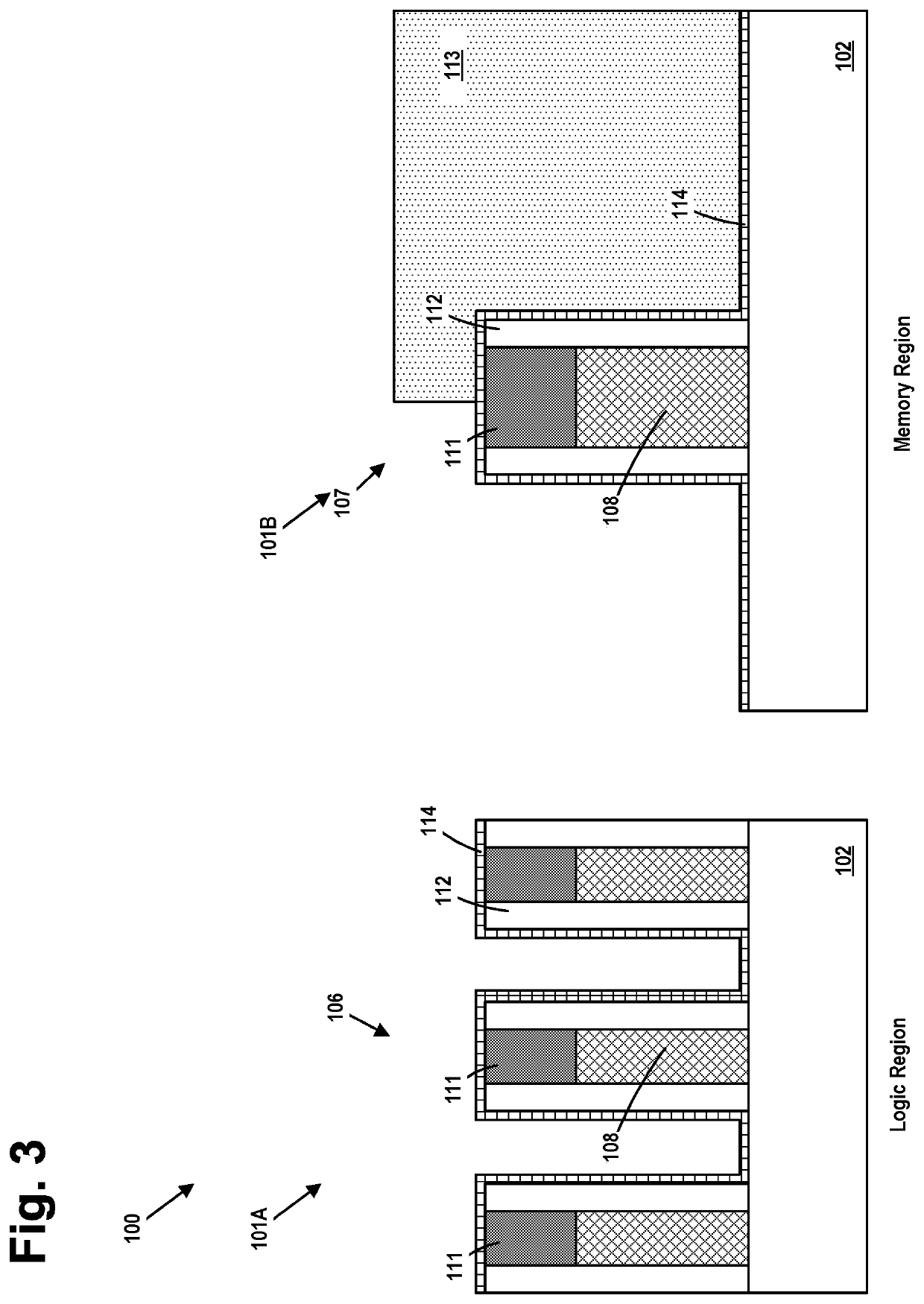
[0010]Various illustrative embodiments of the invention are described below. In the interest of clarity, not all features of an actual implementation are described in this specification. It will of course be appreciated that in the development of any such actual embodiment, numerous implementation-specific decisions must be made to achieve the developers' specific goals, such as compliance with system-related and business-related constraints, which will vary from one implementation to another. Moreover, it will be appreciated that such a development effort might be complex and time-consuming, but would nevertheless be a routine undertaking for those of ordinary skill in the art having the benefit of this disclosure.

[0011]The present subject matter will now be described with reference to the attached figures. Various structures, systems and devices are schematically depicted in the drawings for purposes of explanation only and so as to not obscure the present disclosure with details ...


PUM


Abstract

One illustrative integrated circuit (IC) product disclosed herein includes a selection gate electrode and a first gate insulation layer positioned above a substrate and a memory gate electrode positioned above the substrate and adjacent the selection gate electrode, wherein the memory gate electrode comprises a bottom surface and first and second opposing sidewall surfaces. This embodiment of the IC product also includes a plurality of layers of insulating material, wherein a first portion of the layers of insulating material is positioned between the first gate insulation layer and the first opposing sidewall of the memory gate electrode, a second portion of the layers of insulating material is positioned between the bottom surface of the memory gate electrode and the upper surface of the semiconductor substrate, and a third portion of the layers of insulating material is positioned on the second opposing sidewall of the conductive memory gate electrode.

Description

BACKGROUNDField of the Invention[0001]The present disclosure generally relates to various novel embodiments of a split gate memory device (SG-memory device) such as, for example, a split gate MONOS (Metal Oxide Nitride Oxide Semiconductor) device and various novel methods of making such an SG-memory device.Description of the Related Art[0002]In modern integrated circuit products, it is becoming more common to embed nonvolatile memory cells and logic-based semiconductor devices, such as microprocessors, together on the same semiconductor substrate (or chip) to increase the overall performance of the IC product. One form of nonvolatile memory cell is known as flash memory cells. One traditional form of such flash memory cell included a separate control gate and a separate floating gate that was positioned vertically below the control gate. A tunnel oxide is positioned between the floating gate and the substrate while another layer of oxide is positioned between the control gate and th...

Claims


Application Information

Patent Timeline
IPC IPC(8): H01L29/423H01L27/11556H01L27/11582H01L29/51
CPCH01L27/11556H01L27/11582H01L29/42328H01L29/42352H01L29/42364H01L29/51H01L29/42344H01L29/40117H10B43/10H10B43/40H10B41/27H10B43/27
Inventor ZANG, HUIXIE, RUILONGPANDEY, SHESH MANI
Owner GLOBALFOUNDRIES US INC
Why Eureka
Eureka Blog
Learn More