Forward-biased modulator for cryogenic optical readout

a modulator and forward bias technology, applied in non-linear optics, instruments, optics, etc., can solve the problem of reducing the thermal load on the cryostat, reduce the thermal load on the cryostat, and reduce the complexity of the circuitry

Active Publication Date: 2022-11-22
MASSACHUSETTS INST OF TECH
View PDF2 Cites 2 Cited by
  • Summary
  • Abstract
  • Description
  • Claims
  • Application Information

AI Technical Summary

Benefits of technology

[0005]Apparatus and methods for low-voltage, low-power, amplifier-less, optical read-out of devices in a cryogenic environment are described. A forward-biased optical modulator can be directly driven by a cryogenic device to encode a detection signal onto an optical carrier wave, for example. No power-consuming and heat generating amplifier is needed between the cryogenic device and the optical modulator in the cryogenic environment, thus reducing the thermal load on the cryostat and complexity of the circuitry. The resulting encoded signal can be multiplexed with other signals onto a single optical fiber and carried out of the cryogenic environment. The use of an optical fiber further reduces the thermal load on the cryostat, because the optical fiber has lower thermal conductivity than an electrically conductive cable. An optical fiber also permits greater signal bandwidth and higher data transmission speeds than lengthy electrical cables. Hence, scalability to a large number of optical read-out channels is possible for a cryogenic system. The optical read-out apparatus may be used for superconducting sensors, detectors, and quantum computing apparatus.

Problems solved by technology

The use of an optical fiber further reduces the thermal load on the cryostat, because the optical fiber has lower thermal conductivity than an electrically conductive cable.

Method used


Image

  • Forward-biased modulator for cryogenic optical readout
  • Forward-biased modulator for cryogenic optical readout
  • Forward-biased modulator for cryogenic optical readout

Examples


Embodiment Construction

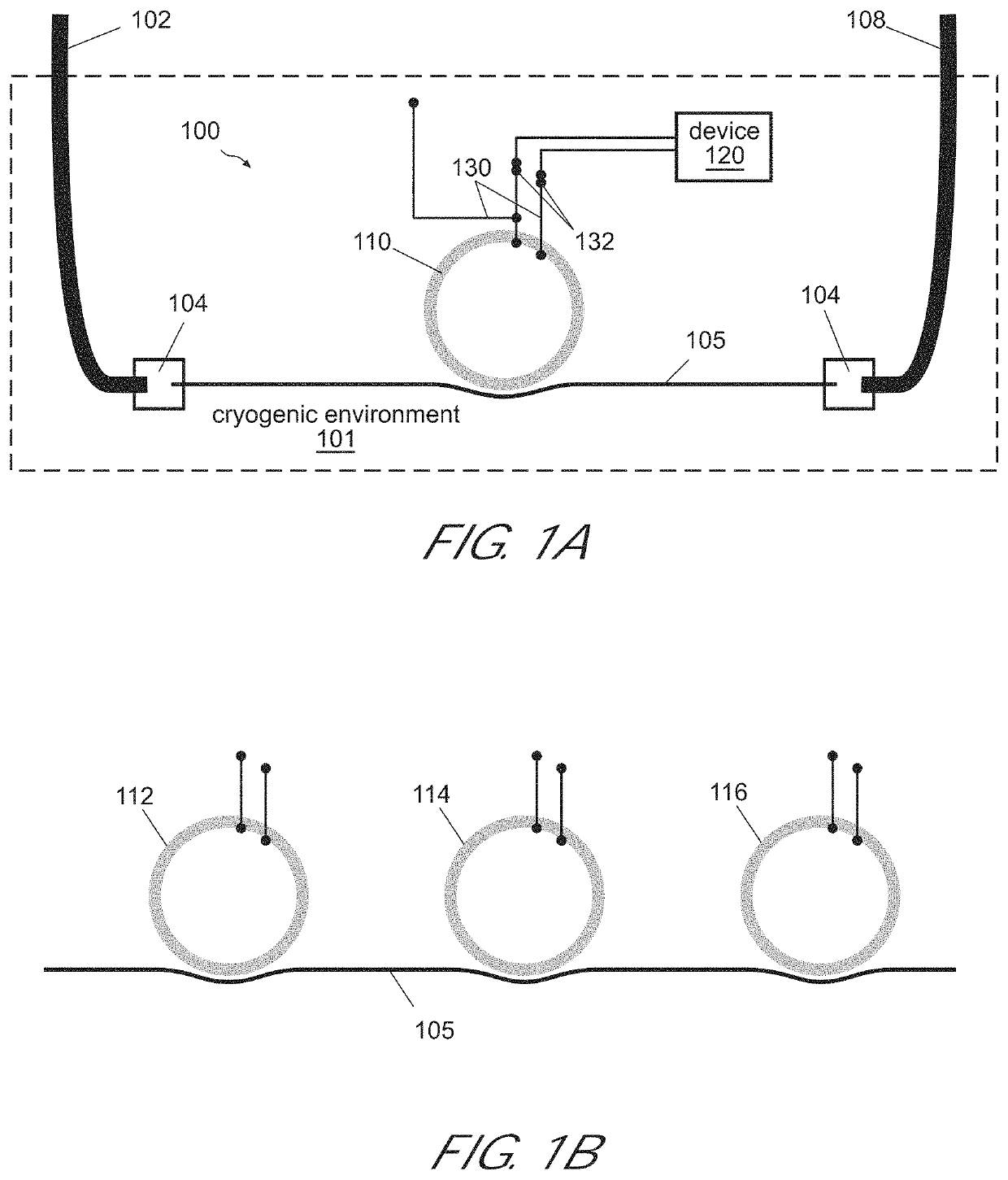
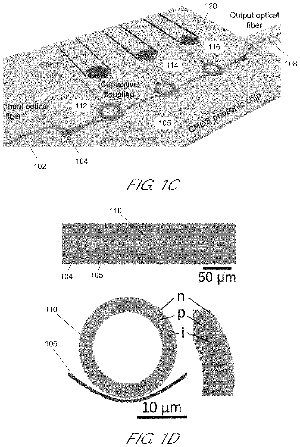
[0038]Most systems operating at cryogenic temperatures communicate with systems operating at room temperature. Conventionally, this transfer of data relies on the use of electrical cables, which have certain disadvantages. Electrical cables present a high heat load to the cryostat due to thermal conduction of the metal wires and the need for amplification inside the cryostat, with milliwatt-scale power dissipation. Electrical cables add long latencies due to the long cable lengths needed to ensure correct thermal anchoring. Also, each electrical cable has a limited bandwidth density, and the cryostat has a limited size so that a large number of cables for handling many signal channels may not be possible.

[0039]The inventors have recognized and appreciated that an alternative approach to cryogenic electrical read-out and data transfer is optical readout and optical data transfer. For example, a signal generated by a cryogenic device in the cryostat is used to drive an electro-optical...


PUM

PropertyMeasurementUnit
temperatureaaaaaaaaaa
resonant wavelengthaaaaaaaaaa

Abstract

Optical read-out of a cryogenic device (such as a superconducting logic or detector element) can be performed with a forward-biased optical modulator that is directly coupled to the cryogenic device without any intervening electrical amplifier. Forward-biasing at cryogenic temperatures enables very high modulation efficiency (1,000-10,000 pm/V) of the optical modulator, and allows for optical modulation with millivolt driving signals and microwatt power dissipation in the cryogenic environment. Modulated optical signals can be coupled out of the cryostat via an optical fiber, reducing the thermal load on the cryostat. Using optical fiber instead of electrical wires can increase the communication bandwidth between the cryogenic environment and room-temperature environment to bandwidth densities as high as Tbps/mm2 using wavelength division multiplexing. Sensitive optical signals having higher robustness to noise and crosstalk, because of their immunity to electromagnetic interference, can be carried by the optical fiber.

Description

CROSS-REFERENCE TO RELATED APPLICATION[0001]The present application claims a priority benefit, under 35 U.S.C. § 119(e), to U.S. provisional application Ser. No. 62 / 957,493 filed on Jan. 6, 2020, titled “Forward-Biased Modulator for Cryogenic Optical Readout,” which application is incorporated herein by reference in its entirety.GOVERNMENT SUPPORT[0002]This invention was made with Government support under Contract No. W911-NF-19-2-0114 awarded by the Army Research Office (ARO) and Contract No. RSA 1615555 awarded by the NASA Jet Propulsion Lab. The Government has certain rights in the invention.BACKGROUND[0003]While promising, optical readout of cryogenic devices is challenging. First, carrier freeze-out (the incomplete ionization of p-type and n-type dopants due to reduced thermal energy) can hinder the performance of semiconductor electro-optic devices operating at cryogenic temperatures. Second, while superconducting devices have low output impedances, typical input impedances fo...

Claims


Application Information

Patent Timeline
Patent Type & Authority Patents(United States)
IPC IPC(8): G02F1/225G02F1/21G02F1/01
CPCG02F1/2257G02F1/0102G02F1/0123G02F1/212G02F2202/10
Inventor RAM, RAJEEV J.GRAY, DODD JOSEPHATABAKI, AMIR H.DE CEA FALCO, MARC
Owner MASSACHUSETTS INST OF TECH
Why Eureka
Try Eureka