Transmission type liquid crystal display having an organic interlayer elements film between pixel electrodes and switching

interlayer element technology, applied in the direction of identification means, instruments, optics, etc., can solve the problems of long time required in the aspect of the fabrication process, the orientation of liquid crystal molecules is affected, and the device is not suitable for a liquid crystal display device requiring high light transmission and transparency

Inactive Publication Date: 2001-06-07
SHARP KK
View PDF0 Cites 40 Cited by
  • Summary
  • Abstract
  • Description
  • Claims
  • Application Information

AI Technical Summary

Problems solved by technology

Therefore, when the pixel electrode 1 is formed on the transparent insulating film, steps will be formed on the pixel electrode 1 if the underlying film has steps, causing disturbance in the orientation of liquid crystal molecules.
This is not suitable for a liquid crystal display device requiring high light transmission and transparency.
Incidentally, in order to obtain a thicker inorganic film made of silicon nitride and the like, an undesirably long time is required in the aspect of the fabrication process.
However, it is not effective for a color display panel for normal notebook type personal computers and the like where pixel electrodes are arranged in a vertical stripe shape (in color display, a square pixel is divided into three vertical...

Method used


Image

  • Transmission type liquid crystal display having an organic interlayer elements film between pixel electrodes and switching
  • Transmission type liquid crystal display having an organic interlayer elements film between pixel electrodes and switching
  • Transmission type liquid crystal display having an organic interlayer elements film between pixel electrodes and switching

Examples


example 3

[0106] (Example 3)

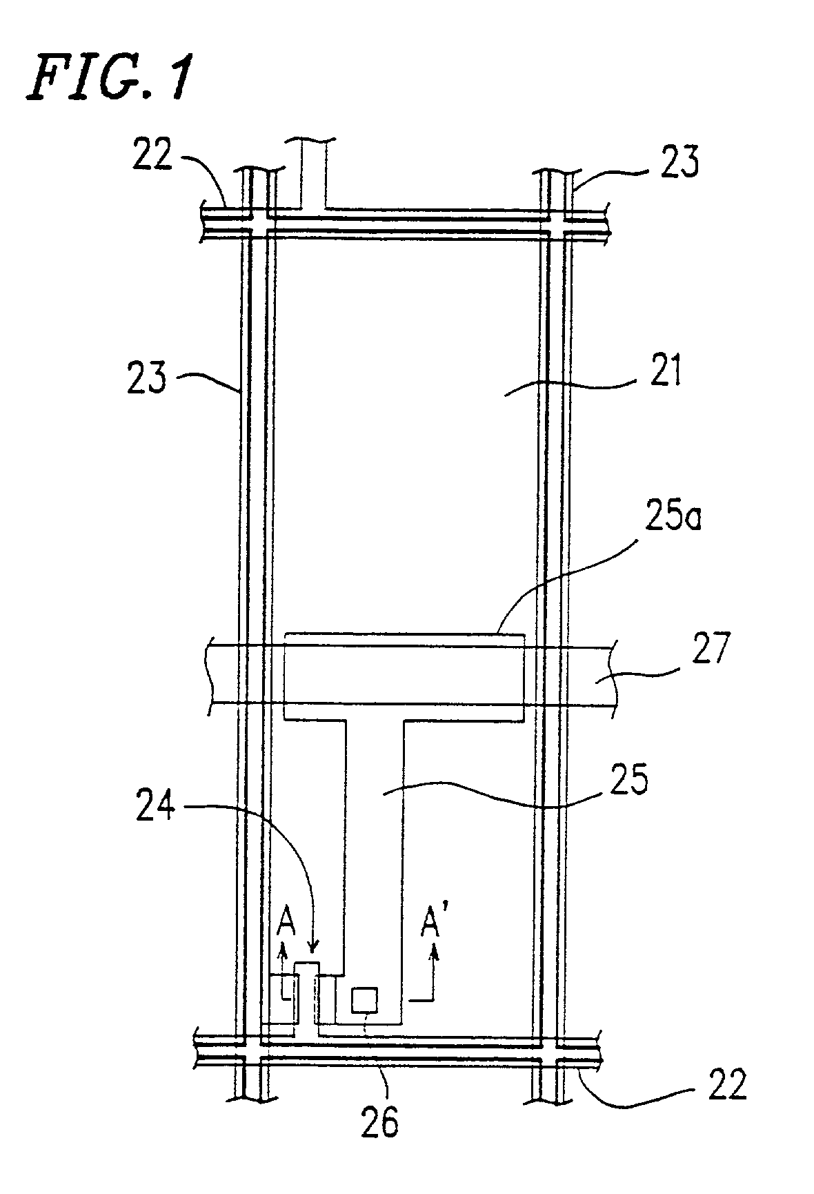
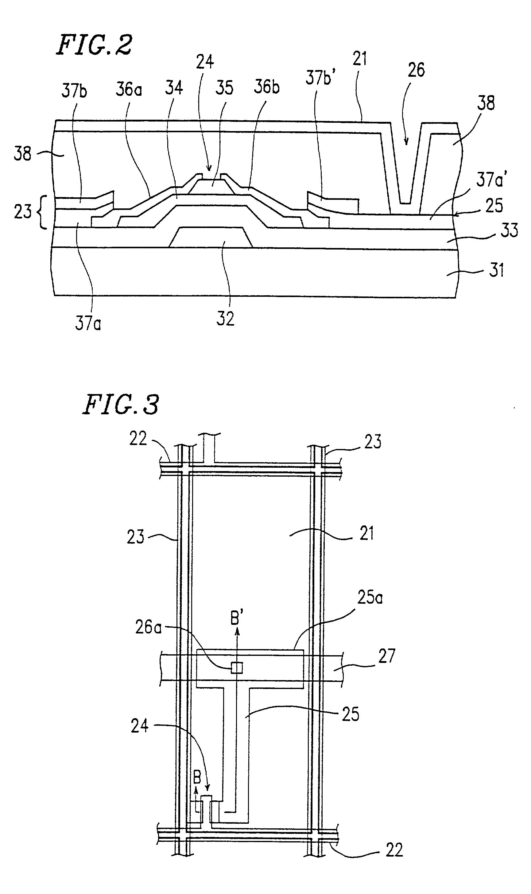
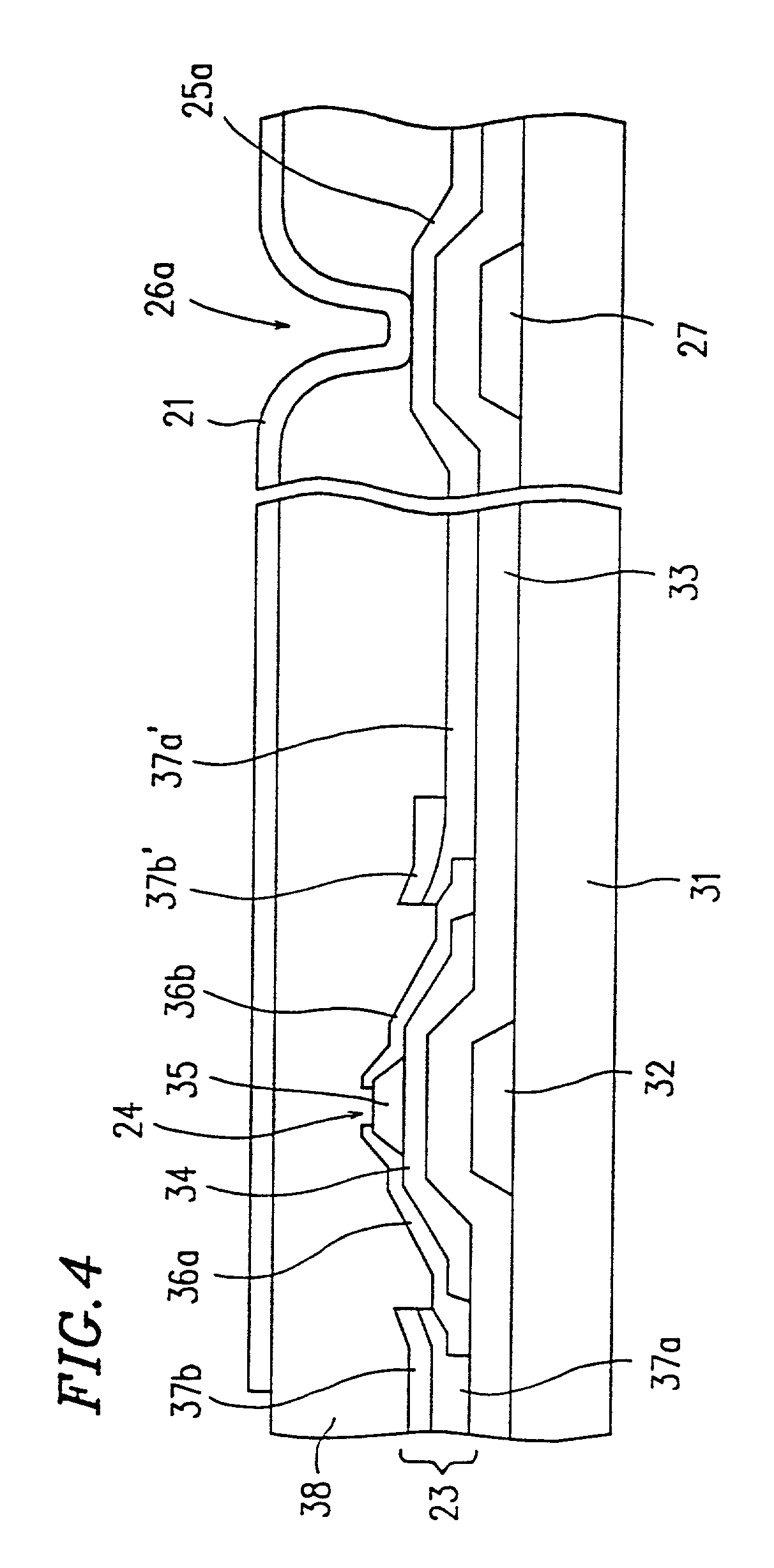
[0107] FIG. 3 is a plan view of a one-pixel portion of an active matrix substrate of the transmission type liquid crystal display device of Example 3 according to the present invention. FIG. 4 is a sectional view taken along line B-B' of FIG. 3. Components having like functions and effects are denoted by the same reference numerals as those in FIGS. 1 and 2, and the description thereof is omitted.

[0108] In the active matrix substrate of this example, each contact hole 26a is formed above the storage capacitor electrode 25a and the storage capacitor counter electrode 27 of the storage capacitor of each pixel. As described in Example 1, the storage capacitor electrode 25a constitutes the end portion of the connecting electrode 25 which is connected to the drain electrode 36b of the TFT 24. The other electrode of the storage capacitor, the storage capacitor counter electrode 27, is connected to a counter electrode formed on a counter substrate via the storage capacito...

example 4

[0113] (Example 4)

[0114] FIG. 5 is a partial sectional view of an active matrix substrate of the transmission type liquid crystal display device of Example 4 according to the present invention. Components having like functions and effects are denoted by the same reference numerals as those in FIGS. 1 to 4, and the description thereof is omitted.

[0115] In the active matrix substrate of this example, each contact hole 26b is formed through the interlayer insulating film 38 above the storage capacitor common line 6. A metal nitride layer 41 is formed on the portion of the transparent conductive film 37a' under each contact hole 26b.

[0116] The above structure of the active matrix substrate of this example is advantageous in the following point.

[0117] Some troubles arise in the adhesion between the resin used for the interlayer insulating film 38 and ITO (indium tin oxide) used for the transparent conductive film or metal such as Ta and Al. For example, in the cleaning process after the ...

example 5

[0119] (Example 5)

[0120] In Example 5, a method for driving the transmission type liquid crystal display device according to the present invention will be described.

[0121] In the transmission type liquid crystal display device according to the present invention, each pixel electrode overlaps the corresponding lines via the interlayer insulating film. If the pixel electrode does not overlap the corresponding lines but gaps are formed therebetween, regions where no electric field is applied are formed in the liquid crystal layer. This trouble can be avoided by overlapping the pixel electrode with the lines. The electric field also is not applied to the regions of the liquid crystal layer corresponding to the boundaries of the adjacent pixel electrodes. However, light leakage which may occur at these regions can be blocked by the existence of lines. This eliminates the necessity of forming a black mask on a counter substrate in consideration of an error at the lamination of the active ...


PUM


Abstract

The transmission type liquid crystal display device of this invention includes: gate lines; source lines; and switching elements each arranged near a crossing of each gate line and each source line, a gate electrode of each switching element being connected to the gate line, a source electrode of the switching element being connected to the source line, and a drain electrode of the switching element being connected to a pixel electrode for applying a voltage to a liquid crystal layer, wherein an interlayer insulating film formed of an organic film with high transparency is provided above the switching element, the gate line, and the source line, and wherein the pixel electrode formed of a transparent conductive film is provided on the interlayer insulating film.

Description

[0001] 1. Field of the Invention[0002] The present invention relates to a transmission type liquid crystal display device which includes switching elements such as thin film transistors (hereinafter, referred to as "TFTs") as addressing elements and is used for displays of computers, TV sets, and the like, and a method for fabricating such a transmission type liquid crystal display device.[0003] 2. Description of the Related Art[0004] FIG. 16 is a circuit diagram of a conventional transmission type liquid crystal display device provided with an active matrix substrate.[0005] Referring to FIG. 16, the active matrix substrate includes a plurality of pixel electrodes 1 arranged in a matrix and TFTs 2 used as switching elements connected to the respective pixel electrodes 1. Gate electrodes of the TFTs 2 are connected to gate lines 3 for supplying a scanning (gate) signal, so that the gate signal can be input into the gate electrodes to control the driving of the TFTs 2. Source electrod...

Claims


Application Information

Patent Timeline
IPC IPC(8): G02F1/1333G02F1/136G02F1/1362G02F1/1368G09F9/30H01L29/786
CPCG02F1/133345G02F1/136209G02F1/136213G02F1/136227G02F2001/13606G02F2201/40G02F1/13606G02F1/1362G02F2201/123H01L29/786
Inventor SHIMADA, TAKAYUKIKAJITANI, MASARUOKAMOTO, MASAYAKONDO, NAOFUMIKATAYAMA, MIKIOSAKUHANA, YOSHIKAZUYAMAMOTO, AKIHIRONAKATA, YUKINOBUNISHIKI, HIROHIKO
Owner SHARP KK
Why Eureka
Try Eureka