Borderless contact structure and method of forming the same

a contact structure and borderless technology, applied in the field of contact structure, can solve the problems degrading electrical characteristics of semiconductor devices, and formation techniques having drawbacks of degrading and achieve the effect of improving contact leakage current characteristics

Inactive Publication Date: 2001-07-26
SAMSUNG ELECTRONICS CO LTD
View PDF1 Cites 30 Cited by
  • Summary
  • Abstract
  • Description
  • Claims
  • Application Information

AI Technical Summary

Benefits of technology

0009] The present invention was made in view of above-mentioned problems and it is a feature of the present invention to provide a borderless contact structure, which improves contact leakage current characteristics.

Problems solved by technology

As a result, the contact resistance between conductive layers, which are electrically connected to each other via contacts, increases to degrade electrical characteristics of the semiconductor device.
However, the conventional borderless contact hole formation technique has a drawback of degrading contact leakage current characteristics due to a recessed device isolation region.
This could lead to the degradation of leakage current characteristics of the semiconductor device.

Method used


Image

  • Borderless contact structure and method of forming the same
  • Borderless contact structure and method of forming the same
  • Borderless contact structure and method of forming the same

Examples


Embodiment Construction

[0027] The preferred embodiment of the present invention will now be described with reference to the accompanying drawings.

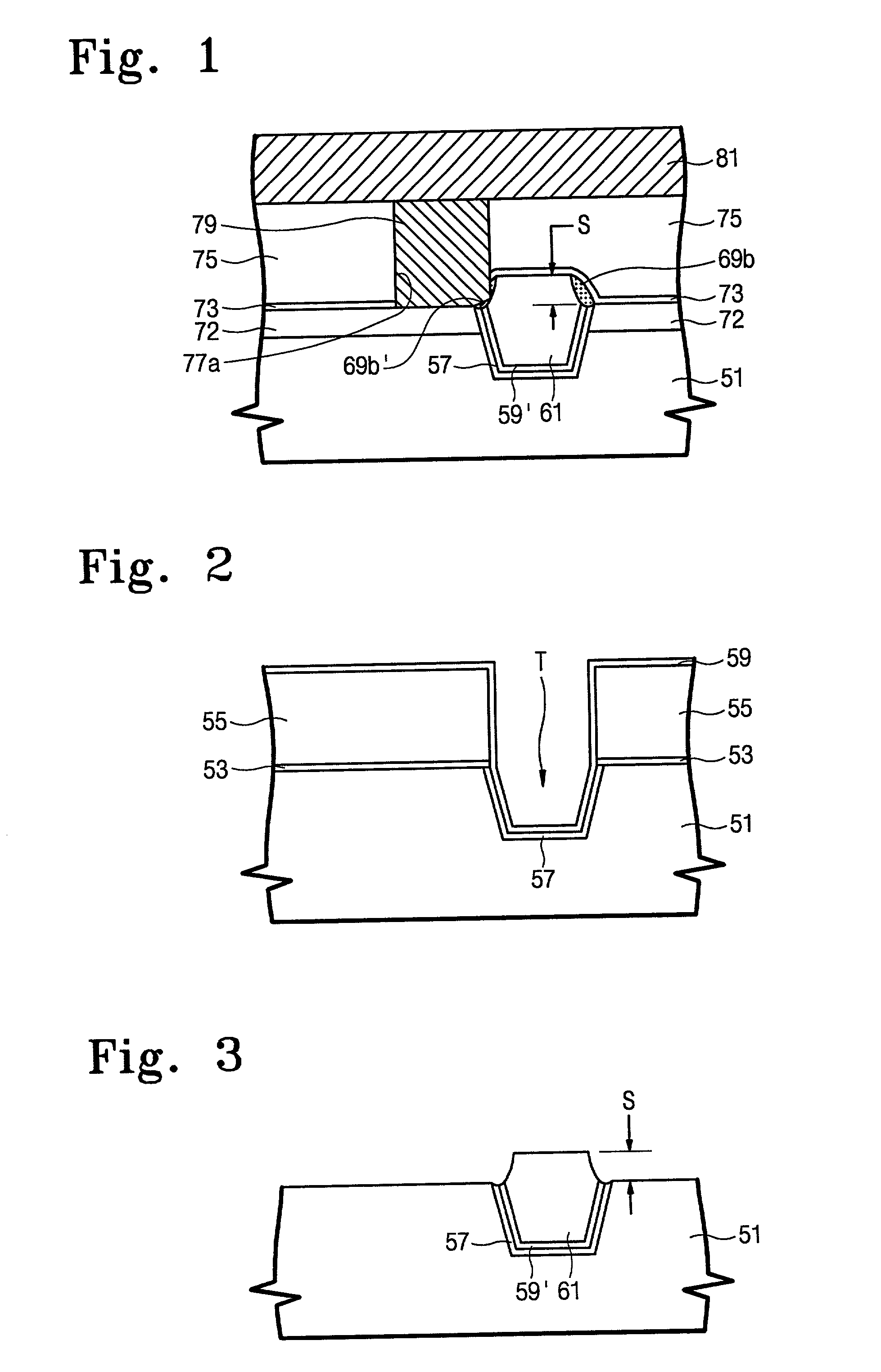
[0028] First, a borderless contact structure according to the present invention will be described with reference to FIG. 1.

[0029] Referring to FIG. 1, a device isolation region 61 such as a trench isolation region is disposed in a predetermined region of a semiconductor substrate 51. The device isolation region 61 can be formed of an insulating material such as a CVD (chemical vapor deposition) oxide layer, and has a protrusion that is higher than the top surface of the semiconductor substrate 51. It is preferable that the step difference S between the semiconductor substrate 51 and the device isolation region 61 is at least 300 angstroms. It is also preferable that a thermal oxide layer 57 is interposed between the substrate 51 and the device isolation region 61. Furthermore, a silicon nitride liner 59' is preferably interposed between the thermal oxide layer 5...


PUM


Abstract

A borderless contact structure and method of forming thereof are provided. A device isolation region having a protrusion is formed at a predetermined region of a semiconductor substrate. The top surface of the protrusion is higher in level than that of the semiconductor substrate. An impurity diffusion region is formed in an active region surrounded by the device isolation region. An etch stop spacer is formed on a sidewall of the protrusion. An etch stop layer and an interlayer insulating layer are sequentially formed on the resultant structure including the impurity diffusion region, the device isolation region and the etch stop spacer. A contact hole opening the interlayer insulating layer and the etch stop layer is formed to expose at least a portion of the impurity diffusion region. Accordingly, during the etching process for forming the borderless contact hole exposing both the impurity diffusion region and the device isolation region adjacent to the impurity diffusion region, the device isolation region adjacent to the impurity diffusion region is not recessed, thereby improving leakage current characteristics of the semiconductor device.

Description

[0001] This application relies for priority upon Korean Patent Application No. 2000-02901, filed on Jan. 21, 2000, the contents of which are herein incorporated by reference in their entirety.BACKGROUND OF THE INVENTION[0002] 1. Field of the Invention[0003] The present invention relates to a contact structure in semiconductor device and method of forming the same and, more particularly, to a borderless contact structure and a method of forming the same.[0004] 2. Description of the Related Art[0005] As the integration density of semiconductor device increases, the size of a contact hole becomes smaller. As a result, the contact resistance between conductive layers, which are electrically connected to each other via contacts, increases to degrade electrical characteristics of the semiconductor device.[0006] Recently, a borderless contact hole formation technique has been proposed as an effort to minimize the contact resistance. The borderless contact hole exposes both a narrow active ...

Claims


Application Information

Patent Timeline
Patent Type & Authority Applications(United States)
IPC IPC(8): H01L21/60H01L21/762H01L21/76
CPCH01L21/76224H01L21/76897H01L21/76
Inventor HA, HOE-SEONGSONG, JUN-EUI
Owner SAMSUNG ELECTRONICS CO LTD
Why Eureka
Try Eureka