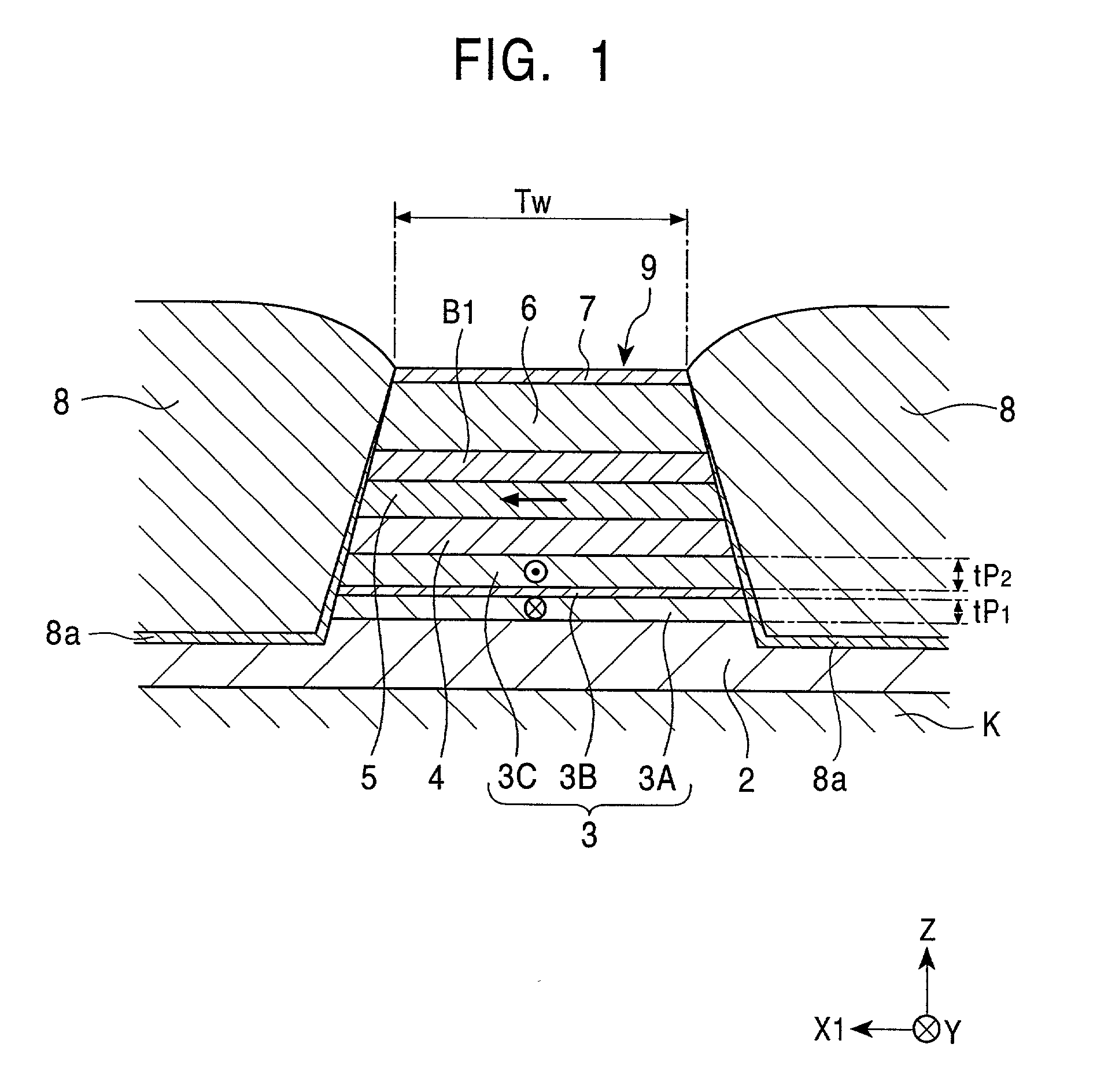
Since the width of the insensitive region varies, it is difficult to precisely define the effective magnetic recording track width.
When the initial magnetic recording track width Tw is set smaller, the rate of change in resistance (.
DELTA.R / R) in the GMR effect decreases, resulting in degradation of the detection sensitivity.
With the degraded detection sensitivity, it is difficult to improve the
recording density.
This is especially problematic because, since the width and the intervals of the recording tracks on the magnetic recording medium are decreased to achieve higher
recording density, the lateral portions 125s may read-out the information on the adjacent track relative to the magnetic recording track which the sensitive region should have had read.
This problem of side-reading may generate
noise in the output signals, causing errors.
Thus, the effective track width cannot be controlled precisely, and the detection precision is degraded.
This is problematic especially in spin-valve thin-film magnetic elements designed for use with magnetic recording track width of 0.5 .mu.m or less.
Such a difference in the free magnetic layer 125 may inhibit the free magnetic layer 125 from being in a single-magnetic-domain state as if there is a
magnetic wall inside, the
magnetization vectors become non-uniform, and Barkhausen
noise may be generated causing
instability and errors in
processing the signals provided from the magnetic recording medium.
An increase in
asymmetry causes degradation in the output characteristics of the spin-valve thin-film magnetic element.
However, these configurations also suffer from the above-described problems.
If the
asymmetry is much larger than zero, the spin-valve thin-film magnetic element cannot exactly read information on a medium.
Thus, the magnetization vector of the free magnetic layer 5 does not change even when there is an external
magnetic field to be detected, the change in resistance does not occur, the detection sensitivity is degraded, and the read output characteristics of the spin-valve thin-film magnetic element are undesirably deteriorated.
Furthermore, the rate of change in resistance cannot be improved by the
spin filter effect which is described below.
In such a case, not only does it become difficult to obtain a large rate of change in resistance (.
DELTA.R / R), but also the exchange anisotropic
magnetic field generated by the exchange
coupling between the free magnetic layer 5 and the
exchange bias layer 6 becomes so weak that it is difficult to control the magnetization vector in the free magnetic layer 5.
Consequently, Barkhausen
noise causing
instability in
processing signals provided from the magnetic recording medium may undesirably occur.
This will lead to a drastic decrease in the effective mean-free-path and to an increased resistance.
(543 K) does not contribute to a further increase in the exchange anisotropic magnetic field of the
exchange bias layer 6 and results in an undesired decrease in magnetoresistive effect due to the thermal interlayer
diffusion.
At a Z content of less than 0.2 atomic percent, ordering of the
crystal lattice in the antiferromagnetic layer is insufficient for yielding a large exchange anisotropic magnetic field.
At an L content of less than 0.2 atomic percent, ordering of the
crystal lattice in the antiferromagnetic layer is insufficient for yielding a large exchange anisotropic magnetic field.
At a Z content of less than 0.2 atomic percent, ordering of the
crystal lattice in the antiferromagnetic layer is insufficient for yielding a large exchange anisotropic magnetic field.
At an L content of less than 0.2 atomic percent, ordering of the crystal lattice in the antiferromagnetic layer is insufficient for yielding a large exchange anisotropic magnetic field.
At a Z content of less than 0.2 atomic percent, the unidirectional exchange
coupling magnetic field is not sufficiently improved.
At a Z content of less than 0.2 atomic percent, the unidirectional exchange
coupling magnetic field is not sufficiently improved.
At a Z content of less than 0.2 atomic percent, the unidirectional exchange coupling magnetic field is not sufficiently improved.
At an L content of less than 0.2 atomic percent, the unidirectional exchange coupling magnetic field is not sufficiently improved.
At an L content of less than 0.2 atomic percent, the unidirectional exchange coupling magnetic field is not sufficiently improved.
At an L content of less than 0.2 atomic percent, the unidirectional exchange coupling magnetic field is not sufficiently improved.
When the Z content exceeds 40 atomic percent, the unidirectional exchange magnetic field undesirably decreases.
When the Z content exceeds 40 atomic percent, the unidirectional exchange magnetic field undesirably decreases.
When the L content exceeds 10 atomic percent, the unidirectional exchange magnetic field undesirably decreases.
When the L content exceeds 10 atomic percent, the unidirectional exchange magnetic field undesirably decreases.
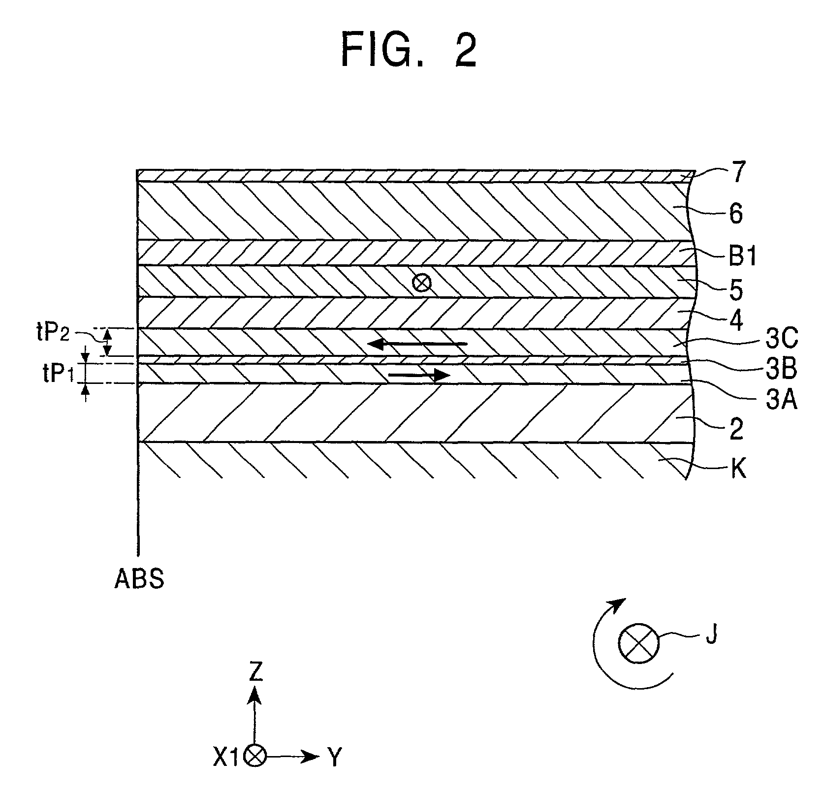
On the other hand, an excess difference in the magnetic thickness between the first pinned magnetic sublayer 3A and the second pinned magnetic sublayer 3C results in an undesired decrease in the exchange coupling magnetic field.
In this case, the magnetization vector of the first pinned magnetic sublayer 3A and the magnetization vector of the second pinned magnetic sublayer 3C are not stabilized in the antiparallel arrangement (ferri-magnetic state), resulting in unstable magnetization states thereof.
At a thickness of the reflective mirror layer S1 exceeding 500 angstroms, the shield gap, that is, the reading gap becomes large, resulting in decreased head resolution.
Thus, it is difficult to control the magnetic domains in the free magnetic layer 5.
As a result, the spin-valve thin-film magnetic element may generate Barkhausen noise, which causes
instability in
signal processing from a magnetic recording medium.
Furthermore, the rate of change in resistance cannot be improved by the
spin filter effect as will be described below.
In such a case, not only it becomes difficult to obtain a large rate of change in resistance (.
DELTA.R / R), but also the exchange anisotropic magnetic field generated by the exchange coupling between the free magnetic layer 5 and the exchange bias layer 6 becomes too weak that it is difficult to control the magnetization vector in the free magnetic layer 5.
Consequently, Barkhausen noise causing instability in processing signals provided from the magnetic recording medium may undesirably occur.
As a consequence, the magnetization vector of the free magnetic layer 15 does not change even when there is an external magnetic field to be detected, the change in resistance does not occur, detection sensitivity is degraded, and the read output characteristics of the spin-valve thin-film magnetic element are undesirably deteriorated.
As a consequence, there is an increased danger that Barkhausen noise is generated causing instability and errors in processing the signals provided form the magnetic recording medium.


