Integrated circuit tester with high bandwidth probe assembly

a probe assembly and integrated circuit technology, applied in the direction of individual semiconductor device testing, waveguides, instruments, etc., can solve the problems of signal distortion, signal attenuation and distortion of signals by impedance discontinuities in the signal path, and it is not possible to reduce the signal path length to zero or to completely eliminate the probe card

Inactive Publication Date: 2001-11-01
FORMFACTOR INC
View PDF0 Cites 9 Cited by
  • Summary
  • Abstract
  • Description
  • Claims
  • Application Information

AI Technical Summary

Problems solved by technology

When those paths carry high frequency test and IC output signals, impedance discontinuities in the signal path can attenuate and distort those signals.
The inherent series inductance and shunt capacitance of the signal routing paths are primary sources of impedance continuities that can lead to signal distortion.
But it is not possible to reduce signal path lengths to zero or to completely eliminate probe card assembly signal path inductance and capacitance.
Thus some level of signal distortion and attenuation is inevitable when signal frequencies are sufficiently high.
Since distortion and attenuation increase with signal frequency, such signal distortion and attention provide a barrier to accurate high frequency testing.

Method used


Image

  • Integrated circuit tester with high bandwidth probe assembly
  • Integrated circuit tester with high bandwidth probe assembly
  • Integrated circuit tester with high bandwidth probe assembly

Examples


Embodiment Construction

)

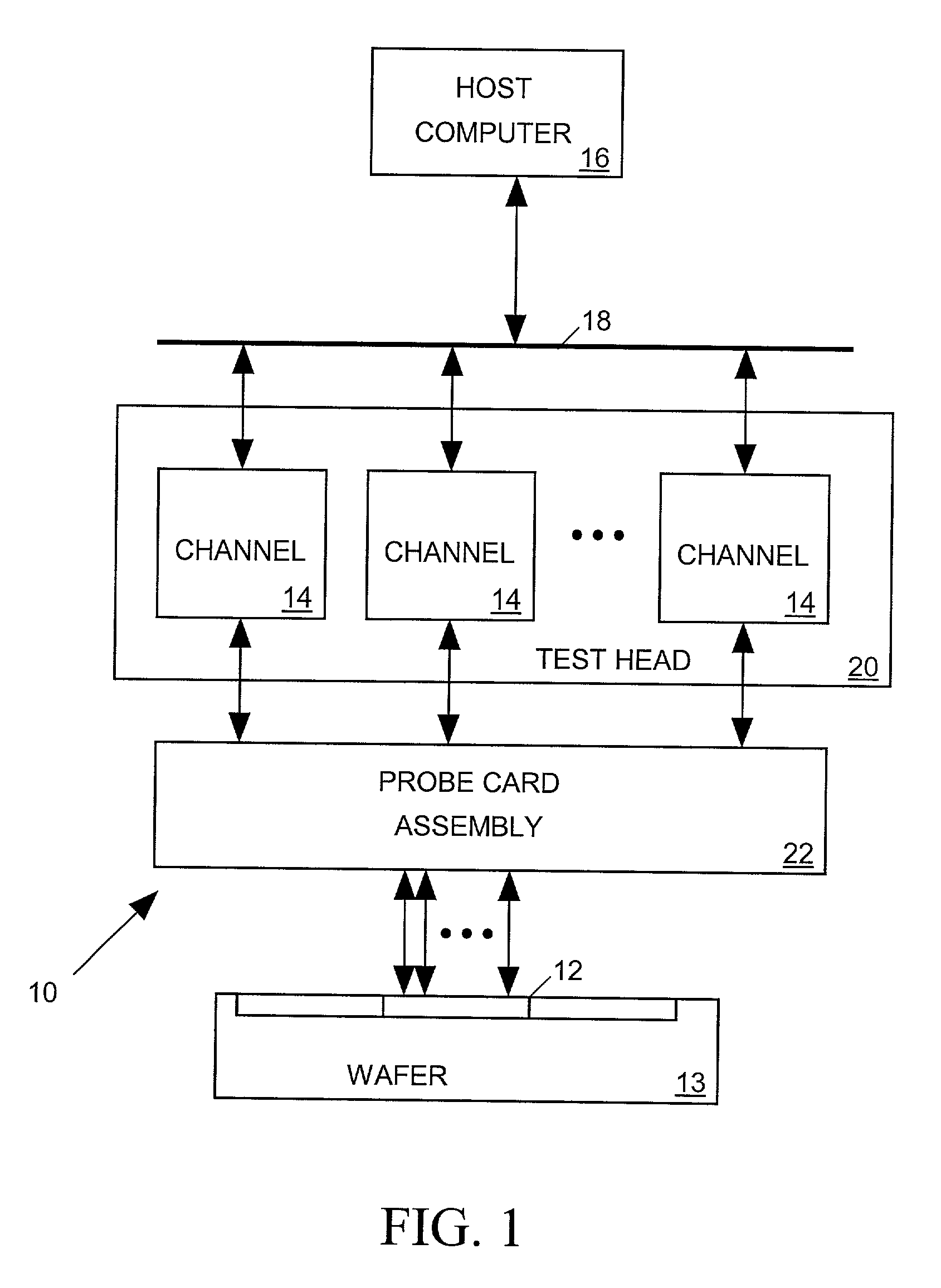
[0022] The present invention relates to integrated circuit (IC) testers and in particular to an improved probe card assembly for conveying signals between bond pads of an integrated circuit device under test (DUT) and the various channels of an IC tester that access the DUT during a test. FIG. 1 illustrates a typical IC tester 10 in block diagram form for performing a test on a DUT 12, suitably in the form of a die on a silicon wafer 13 that has not yet been separated from the wafer and packaged. An IC die typically includes a set of bond pads on its upper surface that are linked to internal circuit nodes and which act as input / output terminals for the IC. The bond pads on a die may provide points of connection for bond wires linking the circuit nodes to pins or legs of an IC package. However when the die is tested before it is packaged, those bond pads may be used as points of contact for probes from the tester for conveying signals between the tester and the internal circuits of ...


PUM


Abstract

Described herein is a probe card assembly providing signal paths for conveying high frequency signals between bond pads of an integrated circuit (IC) and an IC tester. The frequency response of the probe card assembly is optimized by appropriately distributing, adjusting and impedance matching resistive, capacitive and inductive impedance values along the signal paths so that the interconnect system behaves as an appropriately tuned Butterworth or Chebyshev filter.

Description

[0001] The subject matter of the present application is related to that of copending U.S. application FILTER STRUCTURES FOR INTEGRATED CIRCUIT INTERFACES, Ser. No. ______, (Attorney docket No. 1795 (C81)), filed ______, concurrently herewith. The subject matter of the present application is also related to that of copending U.S. application INTEGRATED CIRCUIT INTERCONNECT SYSTEM, Ser. No. ______, (Attorney Docket No. 1796 (C82)) filed concurrently herewith.[0002] 1. Field of the Invention[0003] The present invention relates in general to a probe card assembly for interconnecting test equipment to an integrated circuit die to be tested, and in particular to a probe card assembly that implements each signal path as a high-bandwidth, low-distortion, impedance-matched filter structure between the test equipment and the die.[0004] 2. Description of Related Art[0005] An integrated circuit (IC) die typically includes a set of bond pads on its upper surface acting as input / output terminals ...

Claims


Application Information

Patent Timeline
Patent Type & Authority Applications(United States)
IPC IPC(8): G01R1/067G01R1/073
CPCG01R1/06766G01R1/06772G01R1/073
Inventor MILLER, CHARLES A.
Owner FORMFACTOR INC
Why Eureka
Try Eureka