Monolithic compound semiconductor integrated circuit and method of forming the same

a compound semiconductor, monolithic technology, applied in the direction of semiconductor devices, semiconductor/solid-state device details, electrical devices, etc., can solve the problems of large number of masks and fabrication processes, complicated fabrication processes, and difficulty in accurately controlling resistance values

Inactive Publication Date: 2001-11-22
NEC ELECTRONICS CORP
View PDF2 Cites 38 Cited by
  • Summary
  • Abstract
  • Description
  • Claims
  • Application Information

AI Technical Summary

Problems solved by technology

Such a conventional integrated circuit has the following problems.
This means that the total number of the necessary masks and fabrication processes are large.
This makes the fabrication processes complicated.
A resistance value depends on the shape of the resistance, for which reason it is difficult to accurately control the resistance value.
Further, if another epitaxial base layer underlies the above epitaxial layer, this epitaxial base layer generates a parasitic capacitance, which causes a frequency-dependency of the resistance value.

Method used


Image

  • Monolithic compound semiconductor integrated circuit and method of forming the same
  • Monolithic compound semiconductor integrated circuit and method of forming the same
  • Monolithic compound semiconductor integrated circuit and method of forming the same

Examples


first embodiment

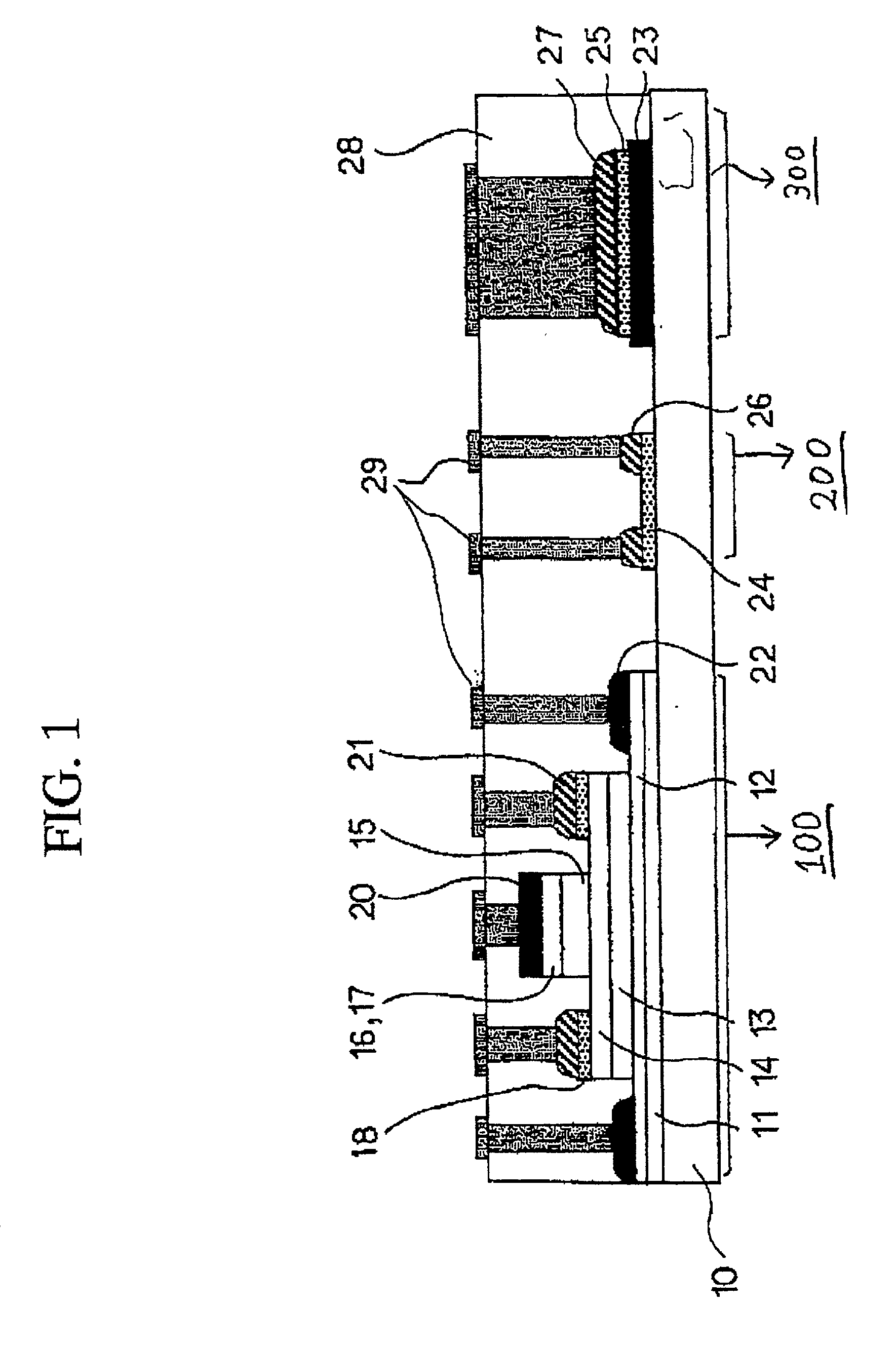
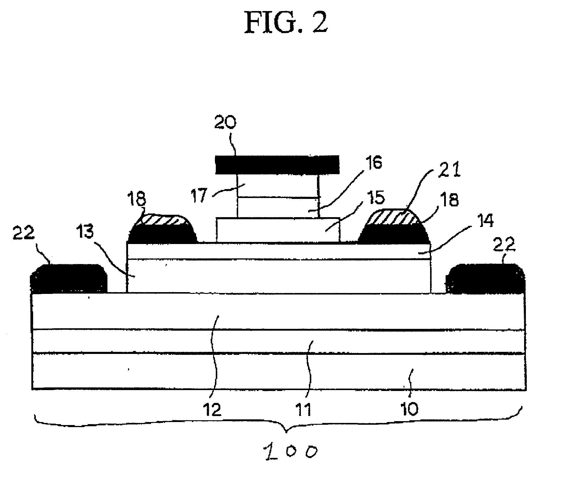
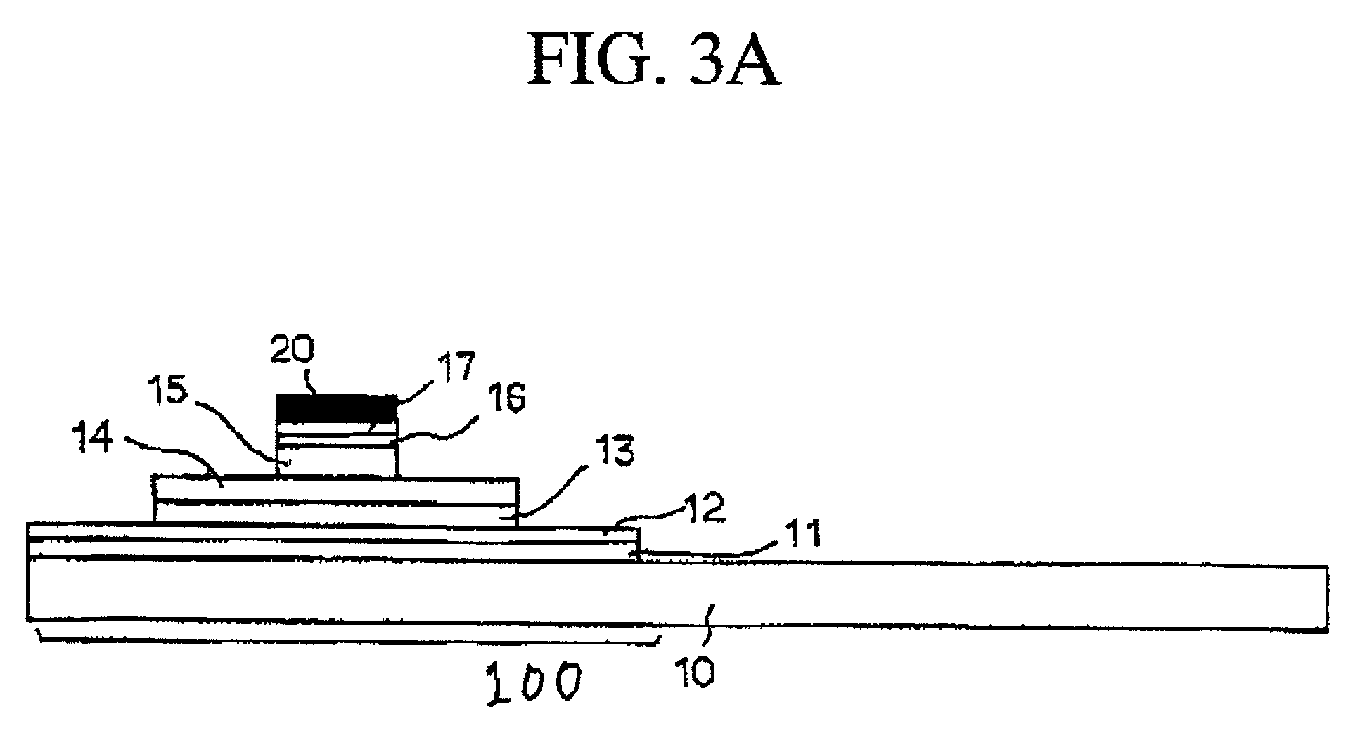
[0068] A first embodiment according to the present invention will be described in detail with reference to the drawings. FIG. 1 is a fragmentary cross sectional elevation view of a monolithic microwave integrated circuit in a first embodiment in accordance with the present invention. A monolithic microwave integrated circuit is provided on a semi-insulating GaAs substrate 10. The monolithic microwave integrated circuit has a monolithic integration of a hetero-junction bipolar transistor 100, a restive element 200 and a metal-insulator-metal capacitor 300.

[0069] The hetero-unction bipolar transistor 100 has an emitter electrode 20, a base electrode 21, and a collector electrode 22. The restive element 200 has a p+-GaAs resistive layer 24 and resistive element electrodes 26. The metal-insulating-metal capacitor 300 has a bottom electrode 23, a p+-GaAs polycrystalline layer 25, and a top electrode 27, wherein the p+-GaAs polycrystalline layer 25 is sandwiched between the top and bottom...

second embodiment

[0103] A second embodiment according to the present invention will be described in detail with reference to the drawings. FIG. 4 is a fragmentary cross sectional elevation view of a monolithic microwave integrated circuit in a second embodiment in accordance with the present invention. A monolithic microwave integrated circuit is provided on a semi-insulating GaAs substrate 10. The monolithic microwave integrated circuit has a monolithic integration of a hetero-junction bipolar transistor 100, a restive element 200 and a metal-insulator-metal capacitor 300.

[0104] The hetero-junction bipolar transistor 100 has an emitter electrode 20, a base electrode 21, and a collector electrode 22. The restive element 200 has a p+-GaAs resistive layer 24 and resistive element electrodes 26. The metal-insulating-metal capacitor 300 has a bottom electrode 23, a p+-GOas polycrystalline layer 25, and a top electrode 27, wherein the p+-GaAs polycrystalline layer 25 is sandwiched between the top and bot...


PUM


Abstract

A monolithically integrated semiconductor device comprises: a hetero-junction bipolar transistor having at least an electrode contact layer which contacts directly with at least one of collector, base and emitter electrodes; and at least a passive device having at least a passive device electrode and at least a resistive layer, wherein the electrode contact layer and the resistive layer comprise the same compound semiconductor layer.

Description

[0001] 1. Field of the Invention[0002] The present invention relates to a compound semiconductor integrated circuit and a method of forming the same, and more particularly to a monolithic microwave integrated circuit which has a monolithic integration of a resistance, a capacitance and a Group III-V compound semiconductor hetero-junction bipolar transistor[0003] 2. Description of the Related Art[0004] As mobile phones and optical communication systems have become widely spread, developments for high frequency and high output devices with reduced noise have become important. A hetero-junction bipolar transistor of a Group III-V compound semiconductor exhibits a superior high frequency performance and a high current driving capability and is operable by a single positive power source. The hetero-junction bipolar transistor is highly attractive. For applying the transistor to the mobile phone, it is necessary to reduce the chip size. In this viewpoint, it is important to develop such a...

Claims


Application Information

Patent Timeline
Patent Type & Authority Applications(United States)
IPC IPC(8): H01L21/28H01L21/331H01L21/822H01L21/8222H01L21/8252H01L23/66H01L27/04H01L27/06H01L29/205H01L29/73H01L29/737
CPCH01L21/8252H01L23/66H01L27/0605H01L29/7371H01L2924/0002H01L2924/00
Inventor FURUHATA, NAOKI
Owner NEC ELECTRONICS CORP
Why Eureka
Try Eureka