

Method and apparatus for high-speed thickness mapping of patterned thin films
a technology of patterned thin films and thickness mapping, which is applied in the field of film thickness measurement, can solve the problems of affecting the efficiency of semiconductor manufacturing, and requiring substantial space in the semiconductor fabrication cleanroom. the rate of semiconductor processing is too slow, and the system is too slow to be used concurrently with semiconductor processing
- Summary
- Abstract
- Description
- Claims
- Application Information
AI Technical Summary
Problems solved by technology
Method used
Image

Examples
first embodiment
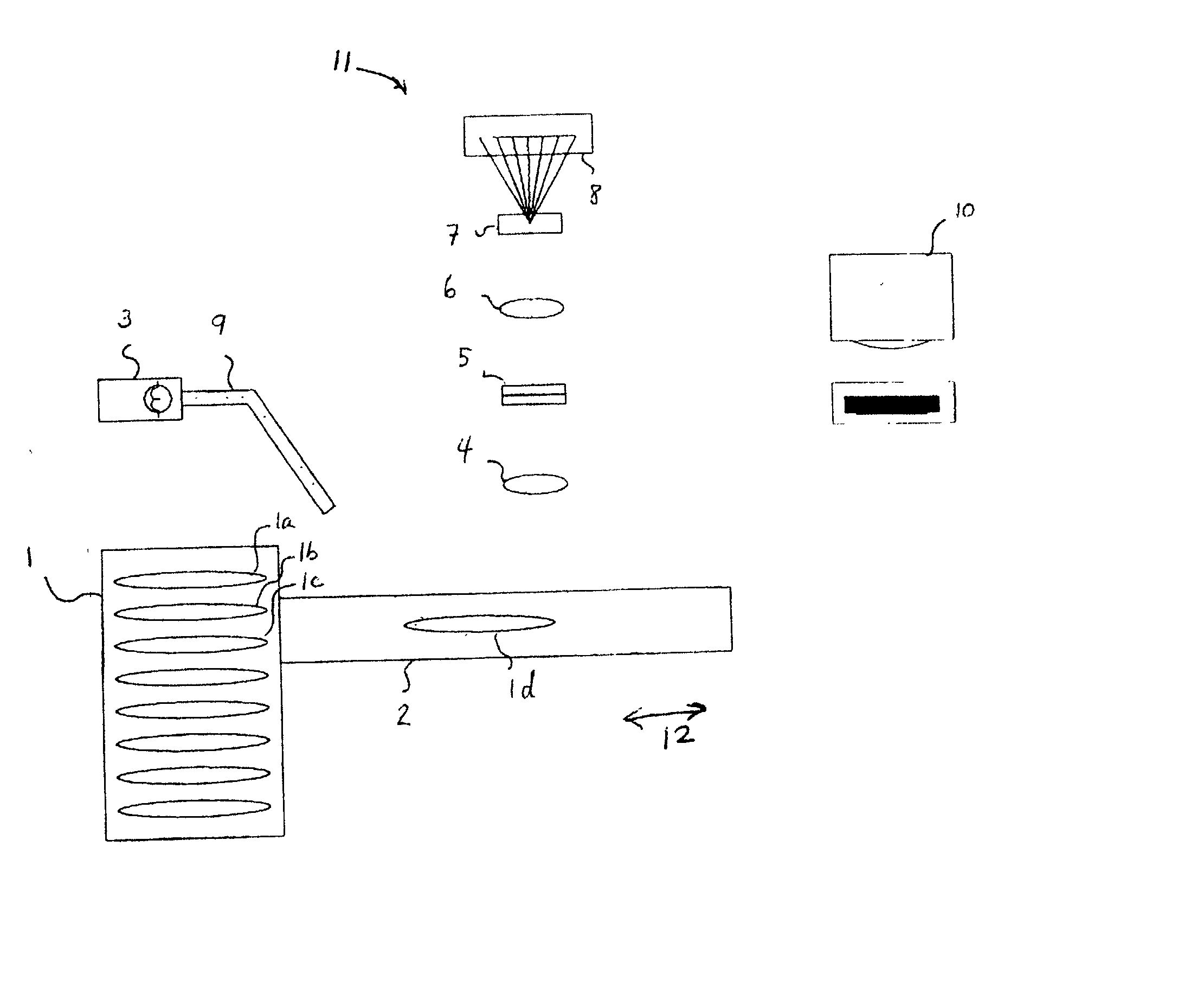
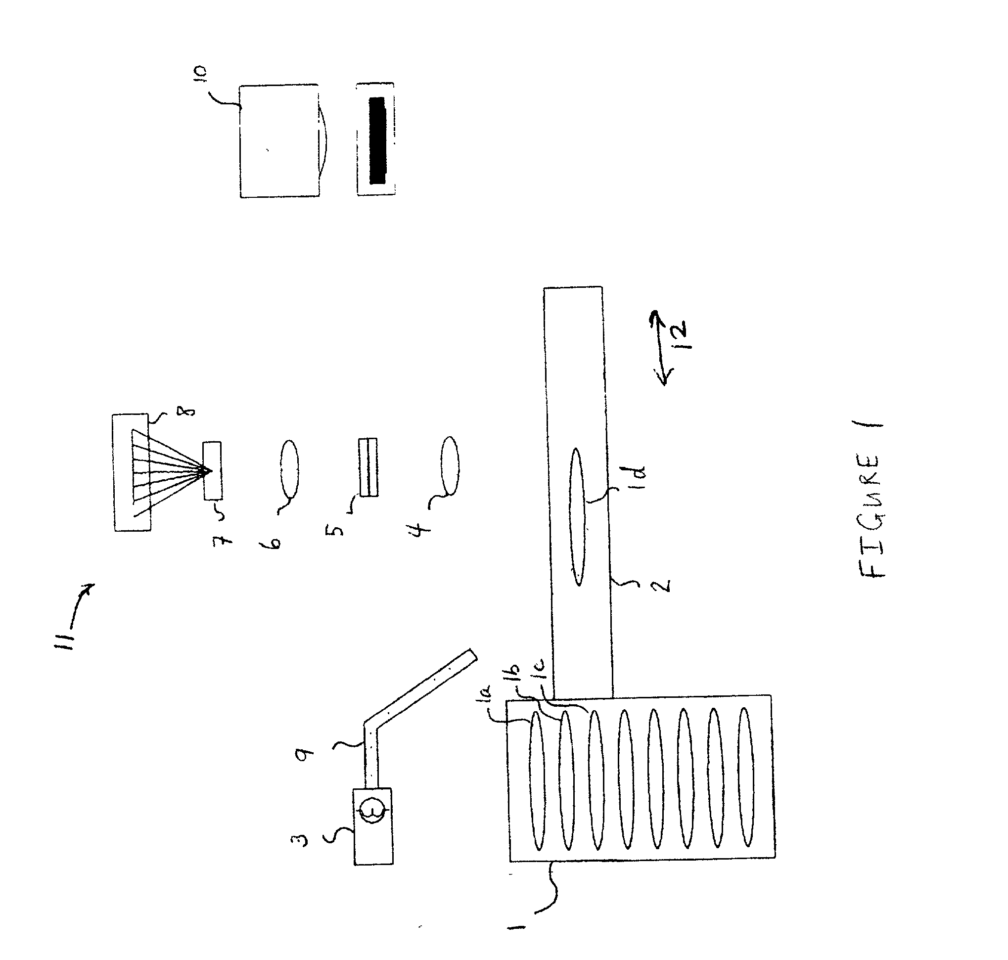
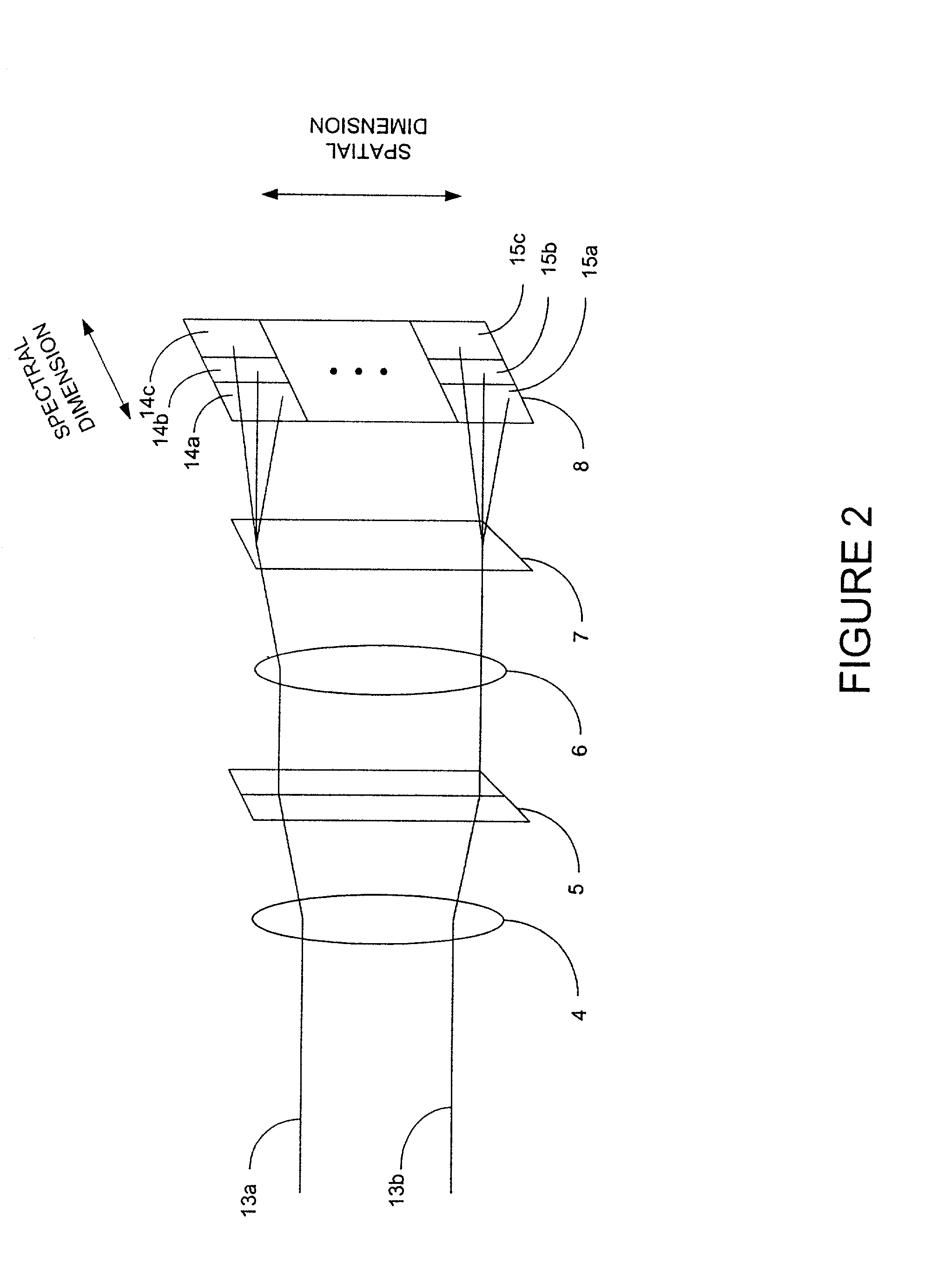
[0033] an imaging system in accordance with the subject invention, suitable for use in applications such as measuring the thickness of transparent or semi-transparent films, is illustrated in FIG. 1. Advantageously, the film to be measured ranges in thickness from 0.001 .mu.m to 50 .mu.m, but it should be appreciated that this range is provided by way of example only, and not by way of limitation. This embodiment is advantageously configured for use with a wafer transfer station 1 to facilitate rapid measurement of a cassette of wafers. The station houses a plurality of individual wafers 1a, 1b, 1c, and is configured to place a selected one of these wafers, identified with numeral 1d in the figure, onto platform 2. This embodiment also comprises a light source 3 coupled to an optical fiber 9 or fiber bundle for delivering light from the light source 3 to the wafer 1d situated on platform 2. Preferably, the light source 3 is a white light source. Advantageously, the light source 3 is...
second embodiment
[0042] the subject invention, suitable for measuring transparent or semi-transparent films, such as dielectrics deposited upon patterned semiconductor wafers, is illustrated in FIG. 3, in which, compared to FIGS. 1-2, like elements are referenced with like identifying numerals. This embodiment is similar to the previous embodiment, with the exception that the wafer id is in a vacuum process or transfer chamber 16, and the wafer motion required for scanning is provided by the transfer robotics 17 that are used to move the wafer inside the process chamber assembly. These transfer robotics allow the wafer 1d to move in the X direction relative to light source 3 and spectrometer 11. Visual access to the wafer 1d is provided by viewport 18. More specifically, light from light source 3 is directed to impinge upon wafer 1d via fiber bundle 9 through viewport 18. In addition, light reflected from wafer 1d is received by spectrometer 11 after passage through viewport 18. As transfer robotics...
examples
[0046] In an example embodiment of the subject invention, suitable for use in a CVD environment, the light source 3 is a tungsten / halogen regulated light source, manufactured by Stocker & Yale, Inc., Salem, N.H.
[0047] Fiber / fiber bundle 9 in this embodiment is a bundle configured into a line of fibers to provide uniform illumination along the measured surface. Such a fiber optic "line light" is manufactured by several companies, Stocker & Yale being a prime example.
[0048] This example is configured for use with CVD processing system Model P5000 manufactured by Applied Materials Inc., Santa Clara, Calif. An optically clear viewport 18 is provided in the standard P5000 configuration.
[0049] The line imaging spectrometer 11 in this example is manufactured by Filmetrics, Inc., San Diego, Calif., the assignee of the subject application. In this spectrometer, the imager 8 is a CCD imager incorporating a time delay and integration line scan camera manufactured by Dalsa Inc., Part No. CT-E4-...
PUM
| Property | Measurement | Unit |
|---|---|---|
| thick | aaaaa | aaaaa |
| thickness | aaaaa | aaaaa |
| thickness | aaaaa | aaaaa |
Abstract
Description
Claims
Application Information