Diamond as a polish-stop layer for chemical-mechanical planarization in a damascene process flow

a technology of damascene and polishing layer, which is applied in the direction of semiconductor devices, semiconductor/solid-state device details, electrical apparatus, etc., can solve the problems of ineffective use of diamond or diamond-like carbon materials as polishing stops, and the addition of topography of the surface of semiconductors, etc., to achieve the effect of greatly improving the thermal conductivity of the finished semiconductor chip

Inactive Publication Date: 2002-04-25
IBM CORP +1
View PDF0 Cites 21 Cited by
  • Summary
  • Abstract
  • Description
  • Claims
  • Application Information

AI Technical Summary

Benefits of technology

[0016] It is another object of the present invention to provide a semiconductor structure having a polish-stop layer material wherein the thermal conductivity of the finished semiconductor chip is greatly improved.
[0017] Another object of the present invention is to provide a method of forming a planarized semiconductor with an improved ability to over-polish during the CMP process without creating additional topography.
[0018] It is another object of the present invention to provide a decrease in the amount of monitoring and control required for the processing of the chemical-mechanical polishing.
[0021] In a preferred embodiment of the present invention discloses a method of planarizing a semiconductor by forming a first diamond-like carbon polish stop layer on a surface of a substrate, forming a second hard-mask layer on the surface of said first polish stop layer, wherein in addition to such second layer being a hard-mask, it further comprises a second polish stop layer, patterning the second layer to form a first set of openings, patterning an exposed portion of the first layer to form a second set of openings, and then patterning an exposed portion of the substrate to form a third set of openings. Thereafter, a third layer is formed on the surface of the substrate therein at least filling the third set of openings and subsequently the substrate surface is planarized to remove at least any excess of the third layer. The planarization may at least stop at the second hard-mask polish-stop to achieve an overall substantial planarity, or may continue to the diamond or diamond-like polish stop layer. The diamond or diamond-like polish stop layer allows for an over-polishing process while still maintaining a substantially planar surface of the substrate.

Problems solved by technology

However, the use of such polish-stop layers must be closely monitored otherwise over-polishing may occur, resulting in additional topography of the surface of the semiconductor.
However, no known art reports the use of diamond or a diamond-like carbon material as a polish-stop layer in patterning a metal layer into an inter-level in a Damascene process.
The use of diamond or a diamond-like carbon material as disclosed in Jaso would not be effective as a polish-stop layer in a patterning step of a Damascene process, primarily due to the volatility of diamond or a diamond-like carbon material during such patterning step.

Method used


Image

  • Diamond as a polish-stop layer for chemical-mechanical planarization in a damascene process flow
  • Diamond as a polish-stop layer for chemical-mechanical planarization in a damascene process flow
  • Diamond as a polish-stop layer for chemical-mechanical planarization in a damascene process flow

Examples


Embodiment Construction

)

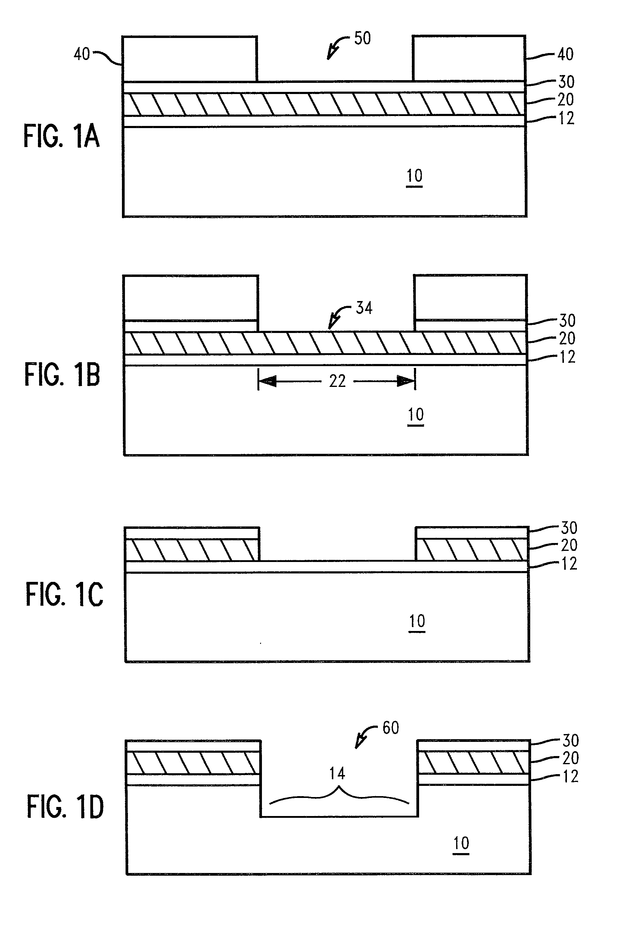
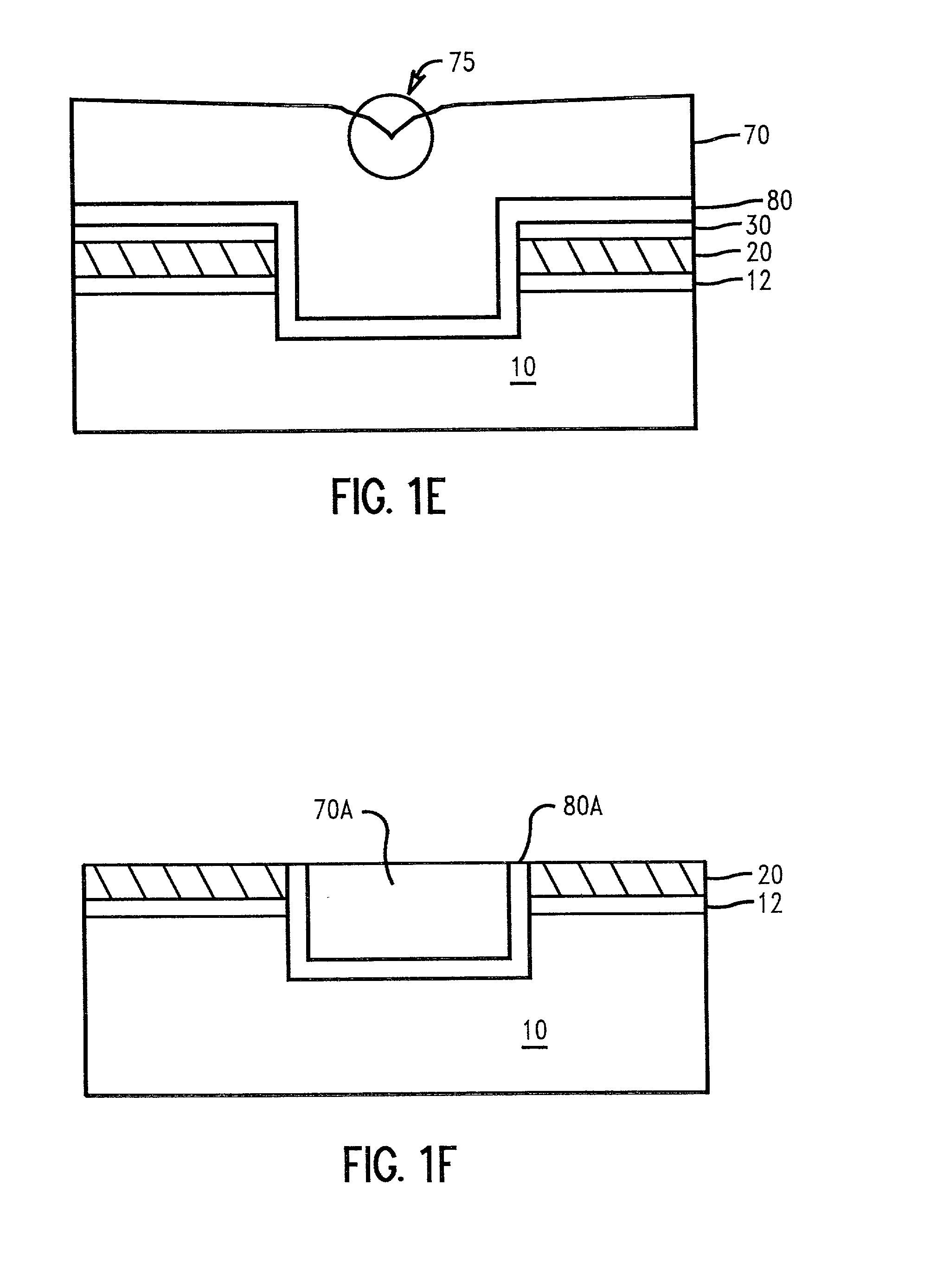
[0030] In describing the preferred embodiment of the present invention, reference will be made herein to FIGS. 1A-3D of the drawings in which like numerals refer to like features of the invention. Features of the invention are not necessarily shown to scale in the drawings. Numerous embodiments of the present invention are possible, including the embodiments described below.

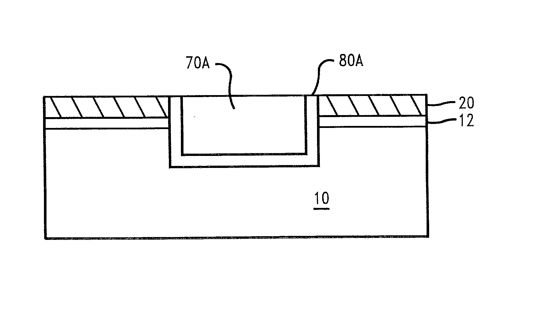
[0031] The present invention discloses the use of diamond or a diamond-like material as a polish-stop layer to pattern and create a semiconductor surface in a Damascene process flow. The present invention may be used to create a variety of planarized semiconductor structures, such as multi-level metal interconnect structure, a semiconductor islands, and shallow trench isolation structures, for example. Generally, the present invention discloses a planarized semiconductor as well as a method of forming the same in a Damascene. Such method comprises optionally depositing a dielectric or conductive layer on the sur...


PUM

PropertyMeasurementUnit
thicknessaaaaaaaaaa
thicknessaaaaaaaaaa
depthaaaaaaaaaa

Abstract

A method of using diamond or a diamond-like carbon layer as a polish-stop for patterning a metal level into an inter-level dielectric substrate using a damascene process flow. The diamond or diamond-like carbon layer is deposited onto the surface of the substrate before patterning the metal level. A protective layer is then deposited over the diamond or diamond-like carbon polish-stop layer, wherein such protective layer may act as an additional polish-stop layer. Together, the diamond or diamond-like carbon polish-stop layer and the protective layer are used as a hard-mask for patterning the trenches that will become the metal features, wherein such protective layer protects the diamond or diamond-like carbon polish-stop layer during the patterning process. After deposition of a conductive metal layer, the dielectric substrate is polished to remove excess conductive material, as well as topography. In the polishing process, the diamond or diamond-like carbon polish-stop layer and any remaining protective layer are used as polish-stop layers. The diamond or diamond-like carbon polish-stop layer allows for an improved planar surface, thereby resulting in an sufficient decrease in topography at the surface of the inter-level dielectric.

Description

[0001] 1. Field of the Invention[0002] The present invention relates to planarizing semiconductor devices in a Damascene process, and more particularly, to methods of planarizing a variety of surfaces of semiconductor devices by using first a diamond or a diamond-like carbon layer as a polish-stop layer, and then protecting such diamond-like carbon layer with a hard-mask, wherein such hard-mask may act as an additional polish-stop layer, thereafter chemically-mechanically polishing the surface of such semiconductor thereby producing an improved planarized surface.[0003] 2. Description of Related Art[0004] Semiconductor devices can be patterned by a variety of methods, as disclosed in the prior art. A Damascene process flow is one such technique. Typically, a Damascene process comprises depositing an insulator material onto the surface of a substrate, patterning the insulator material to form openings for wires and vias, depositing a conductive material, generally a metal, into such ...

Claims


Application Information

Patent Timeline
Patent Type & Authority Applications(United States)
IPC IPC(8): H01L21/76H01L21/285H01L21/304H01L21/306H01L21/308H01L21/3105H01L21/311H01L21/3205H01L21/321H01L21/762H01L21/768
CPCH01L21/28525H01L21/3081H01L21/7684H01L21/31144H01L21/3212H01L21/31053
Inventor CLEVENGER, LAWRENCE A.HSU, LOUIS L. C.STEPHENS, JEREMY K.WISE, MICHAEL
Owner IBM CORP
Why Eureka
Try Eureka