RF power device and method of manufacturing the same

a technology of power devices and manufacturing methods, applied in semiconductor devices, semiconductor/solid-state device details, electrical apparatus, etc., can solve problems such as difficulty in fabricating devices and reducing hf characteristics of power devices

Inactive Publication Date: 2002-05-09
ELECTRONICS & TELECOMM RES INST
View PDF0 Cites 32 Cited by
  • Summary
  • Abstract
  • Description
  • Claims
  • Application Information

AI Technical Summary

Problems solved by technology

Such structure seriously causes an unnecessary lateral diffusion owing to the diffusion for a long time, thus an area of the device becomes large, and a parasitic resistance and a parasitic capacitance are increased by such result, which is an important cause of reducing an HF characteristic of the power device.
Furthermore, the conventional LDMOS str

Method used


Image

  • RF power device and method of manufacturing the same
  • RF power device and method of manufacturing the same
  • RF power device and method of manufacturing the same

Examples


Embodiment Construction

[0023] Hereinafter, preferred embodiments of the present invention will be described in detail with reference to the accompanying drawings.

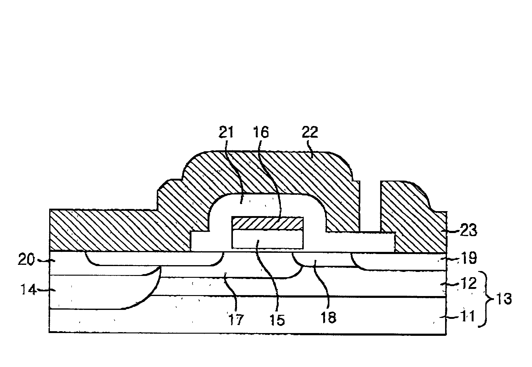
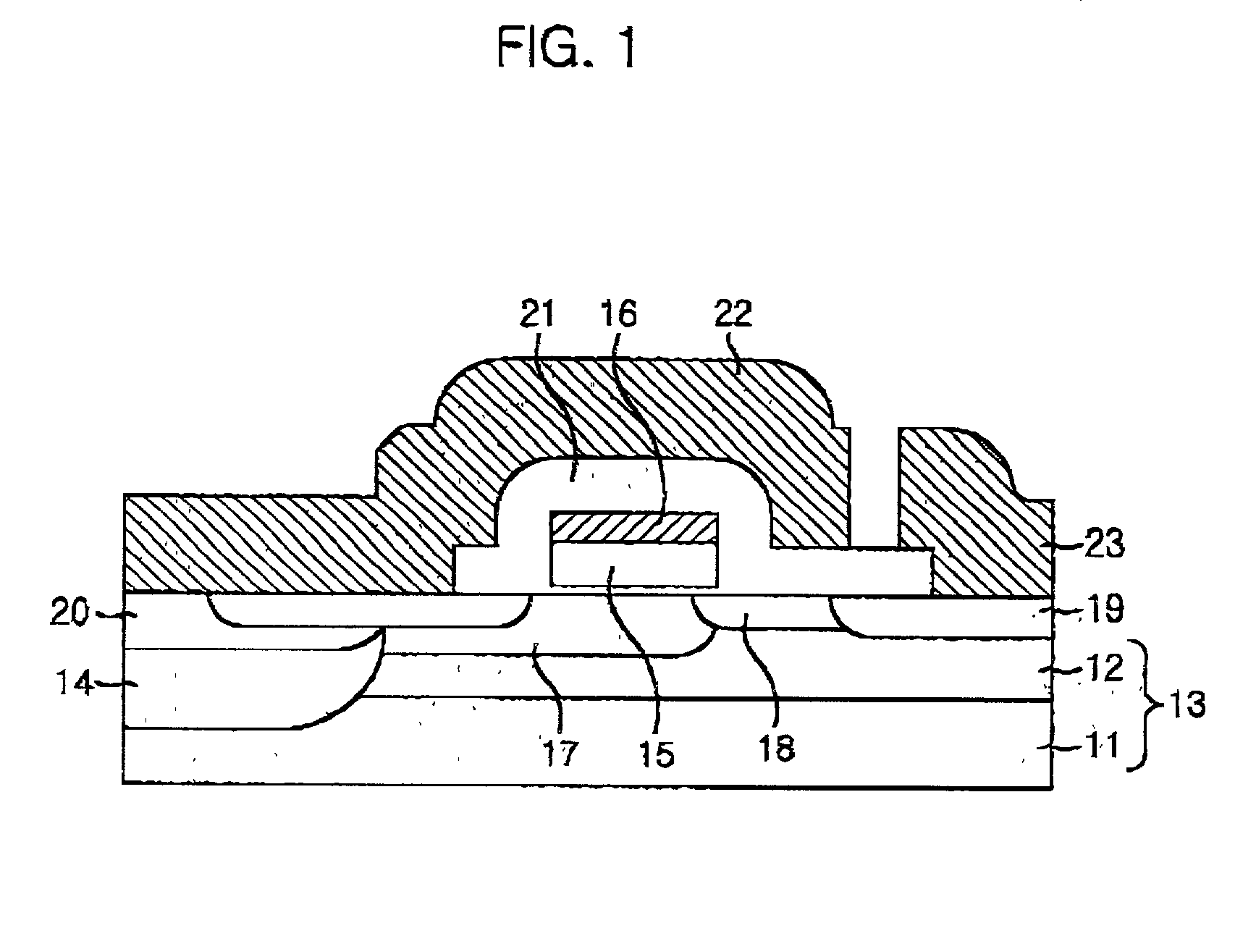
[0024] FIG. 2 is a structural plane view of an HF power device in a first embodiment of the present invention. In FIG. 2, it is formed source electrode 51 wide in comparison with drain electrode 52, and a P.sup.-doping layer 36a of a column shape and a P.sup.- sinker 37 (of FIG. 3) formed by a poly-silicon column 36b are connected to a center portion of a lower part of the source electrode 51. Herewith, the P.sup.-poly-silicon column 36b is buried into numerous trenches or into one trench, and the P.sup.- doping layer 36a is formed on the neighborhood of one or numerous trenches.

[0025] Both sides of the P.sup.- sinker 37 are connected with N.sup.+ source areas 47 of adjacent devices, in other words, the P.sup.- sinker 37 is formed commonly in the adjacent devices, and the P.sup.- sinker 37 and the N.sup.+ source areas 47 of the mutually adjacent ...


PUM


Abstract

An HF power device in an HF transistor includes a semiconductor layer as a first conductive type, a field area formed in a trench structure on one side of the semiconductor layer, gate electrode formed on a given surface of the semiconductor layer, a channel layer as a second conductive type laterally diffused from the field area to a width containing both sides of the gate electrode, and formed on the surface of the semiconductor layer, a source area as the second conductive type formed within the channel layer between one side of the gate electrode and the field area, a drain area as the second conductive type formed on the surface of the semiconductor layer with a given interval from another side of the gate electrode, a sinker as the first conductive type provided as a column shape of a trench structure for dividing into two source areas by a piercing through the source area, and connected to the semiconductor layer, an LDD area as the second conductive type formed on the surface of the semiconductor layer between the drain area and the gate electrode, first metal electrode contacted with the source area divided into two source areas and electrically connected to the semiconductor layer through the sinker, and second metal electrode coupled with the drain area.

Description

[0001] The present invention relates to a high-output power device; and, more particularly, to an HF power device applicable to a power amplifier of a base station for a mobile communication system such as a cellular, a personal communication service (PCS) and an IMT (International Mobile Telecommunication-2000 etc.[0002] In addition, the present invention is relates to an HF power device applicable even to a mobile station based on a little watt in case that a structure of the device becomes scale-down, though it is being applied to a power amplifier of the base station for scores of or hundreds of watt.PRIOR ART OF THE INVENTION[0003] In general, a MOSFET (Metal Oxide Silicon Field Effect Transistor) used as a power device has high input impedance in comparison with a bipolar transistor, thus a power gain is high and a gate driving circuit is very simple. Also the MOSFET is a unipolar device, thus it has a merit that there is less time delay occurring by a re-combination or an acc...

Claims


Application Information

Patent Timeline
IPC IPC(8): H01L29/10H01L29/417H01L29/78
CPCH01L29/1087H01L29/4175H01L29/41766H01L29/7835H01L2924/0002H01L2924/00H01L29/78
Inventor KIM, CHEON-SOOYU, HYUN-KYUHWANG, NAMPARK, JUNG-WOO
Owner ELECTRONICS & TELECOMM RES INST
Why Eureka
Try Eureka