Plasma enhanced chemical processing reactor and method

a technology of enhanced chemical processing and reactor, applied in the direction of chemical vapor deposition coating, coating, electric discharge tube, etc., can solve the problem of difficult to achieve the desired effect, and achieve the effect of improving the quality of films deposited

Inactive Publication Date: 2002-06-27
APPLIED MATERIALS INC
View PDF4 Cites 356 Cited by
  • Summary
  • Abstract
  • Description
  • Claims
  • Application Information

AI Technical Summary

Benefits of technology

[0010] A related object of this invention is to provide a reactor which improves the quality of films deposited on wafers.

Problems solved by technology

These properties become more difficult to attain as device dimensions shrink.

Method used


Image

  • Plasma enhanced chemical processing reactor and method
  • Plasma enhanced chemical processing reactor and method
  • Plasma enhanced chemical processing reactor and method

Examples


Embodiment Construction

[0027] A. Overview

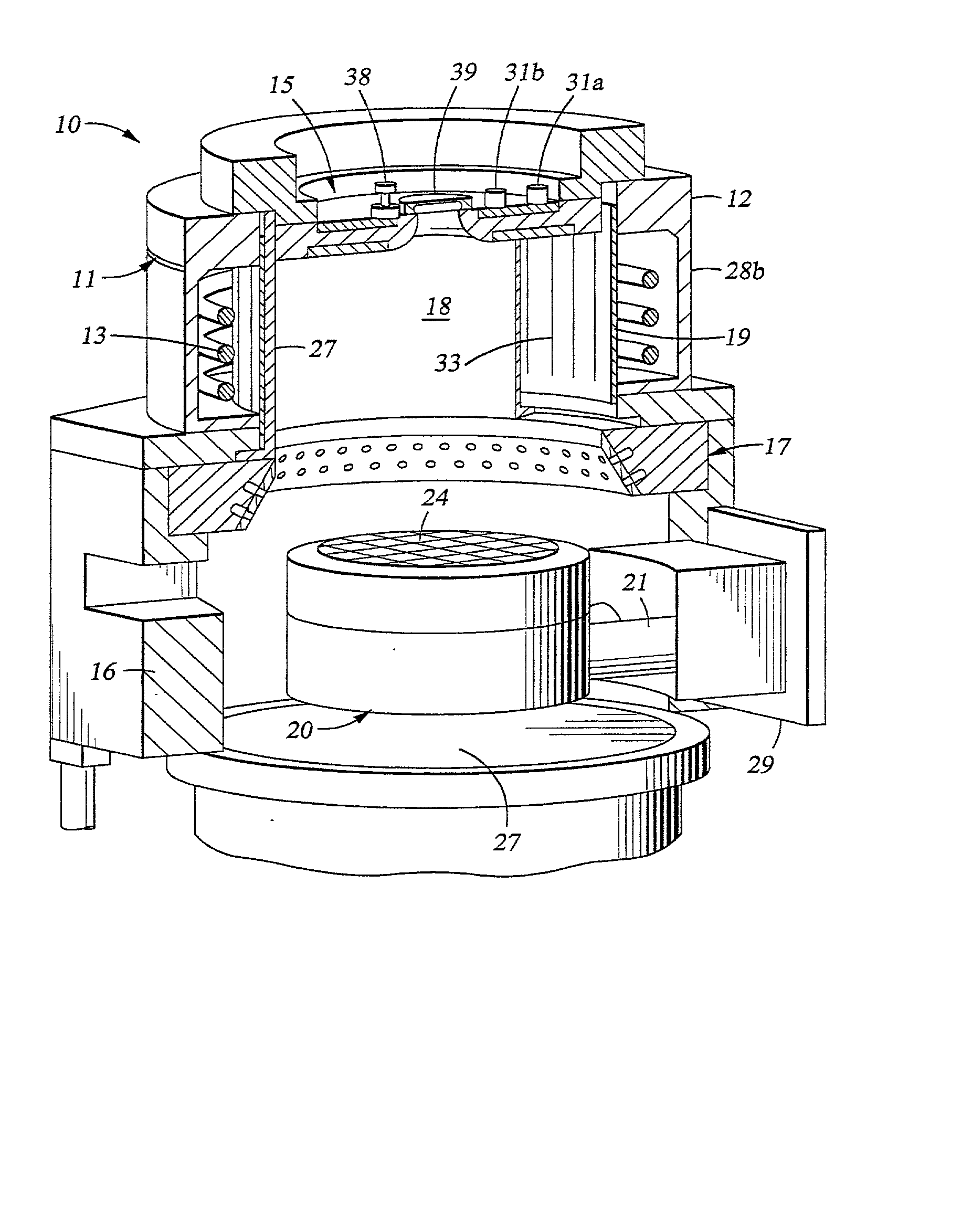
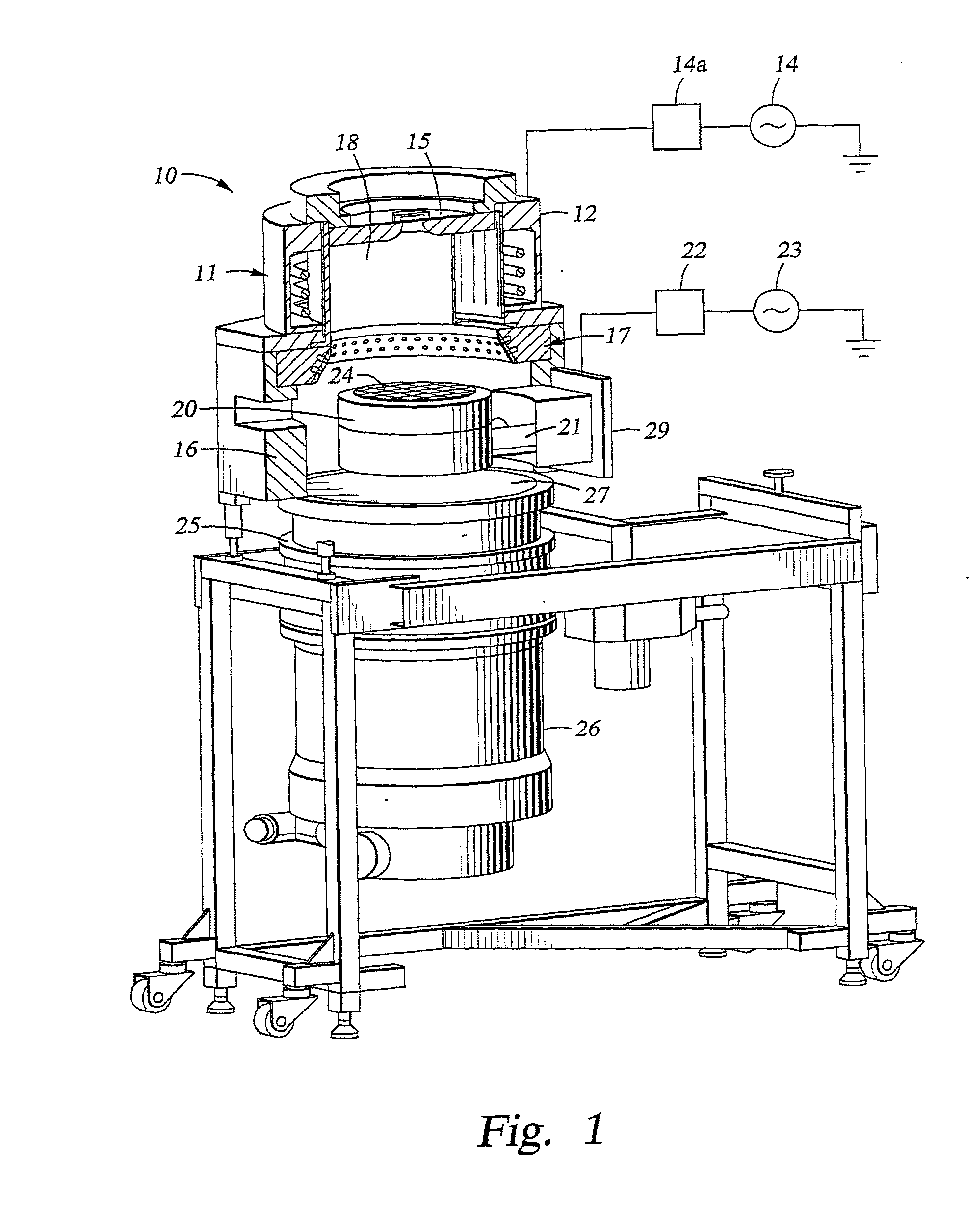
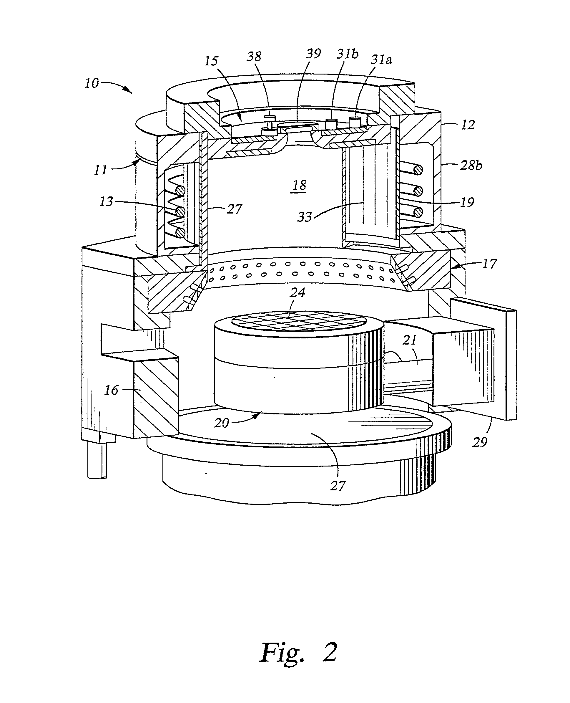
[0028] Turning to the drawings, wherein like components are designated by like reference numbers in the figures, FIGS. 1 and 2 represent one embodiment of the reactor in accordance with this invention. FIG. 1 illustrates an assembly view of the invention wherein reactor 10 generally comprises a plasma assembly 11 and a process chamber 16. The plasma assembly 11 which includes a plasma generating source 12, the interior of such source 12 forms a plasma chamber 18, and a first gas injection manifold 15 forms the top of the chamber. The first manifold 15 conveys at least one gaseous chemical to plasma chamber 18. The plasma assembly 11 is operatively attached to process chamber 16. Process chamber 16 generally includes a second gas injection manifold 17, which is mounted to process chamber 16, for receiving at least a second gaseous chemical via gas delivery lines (not shown). Preferably, the gas injection manifold 17 is mounted near the top of chamber 16 with an oute...


PUM

PropertyMeasurementUnit
frequencyaaaaaaaaaa
pressureaaaaaaaaaa
pressureaaaaaaaaaa

Abstract

A plasma enhanced chemical processing reactor and method. The reactor includes a plasma chamber including a first gas injection manifold and a source of electromagnetic energy. The plasma chamber is in communication with a process chamber which includes a wafer support and a second gas manifold. The plasma generated in the plasma chamber extends into the process chamber and interacts with the reactive gases to deposit a layer of material on the wafer. The reactor also includes a vacuum system for exhausting the reactor. The method includes the steps of generating a plasma within the plasma chamber, introducing at least one gaseous chemical into the process chamber proximate to the wafer support and applying r.f. gradient to induce diffusion of the plasma to the area proximate the wafer support.

Description

[0001] This invention relates to a reactor and method for processing semiconductor integrated circuits. More particularly, the invention relates to a plasma enaanced reactor and method capable of performing processing operations including depositing uniform films or layers on the surface of integrated circuits by plasma enhanced chemical vapor deposition (PECVD), film etchback, reactor self-clean, and simultaneous etch and deposit operations. A[0002] The processing of semiconductor wafers and other integrated circuits (IC) includes critical manufacturing steps such as etching wafer surfaces and depositing layers of material on wafer surfaces to form device components, interconnecting lines, dielectrics, insulating barriers and the like. Various systems have been employed to deposit layers of material and the like on the surface of integrated circuits, and often such layers are formed by chemical vapor deposition (CVD). A conventional thermal CVD process deposits a stable chemical co...

Claims


Application Information

Patent Timeline
Patent Type & Authority Applications(United States)
IPC IPC(8): C23C16/44C23C16/455C23C16/507H01J37/32
CPCC23C16/4558C23C16/463H01J37/3244H01J37/321C23C16/507
Inventor OS, RON VANDURBIN, WILLIAM J.MATTHIESEN, RICHARD H.FENSKE, DENNIS C.ROSS, ERIC D.
Owner APPLIED MATERIALS INC
Why Eureka
Try Eureka