

Precision electroplated solder bumps and method for manufacturing thereof
- Summary
- Abstract
- Description
- Claims
- Application Information
AI Technical Summary
Benefits of technology
Problems solved by technology
Method used
Image

Examples
Embodiment Construction
[0024] 1. The Preferred Embodiments
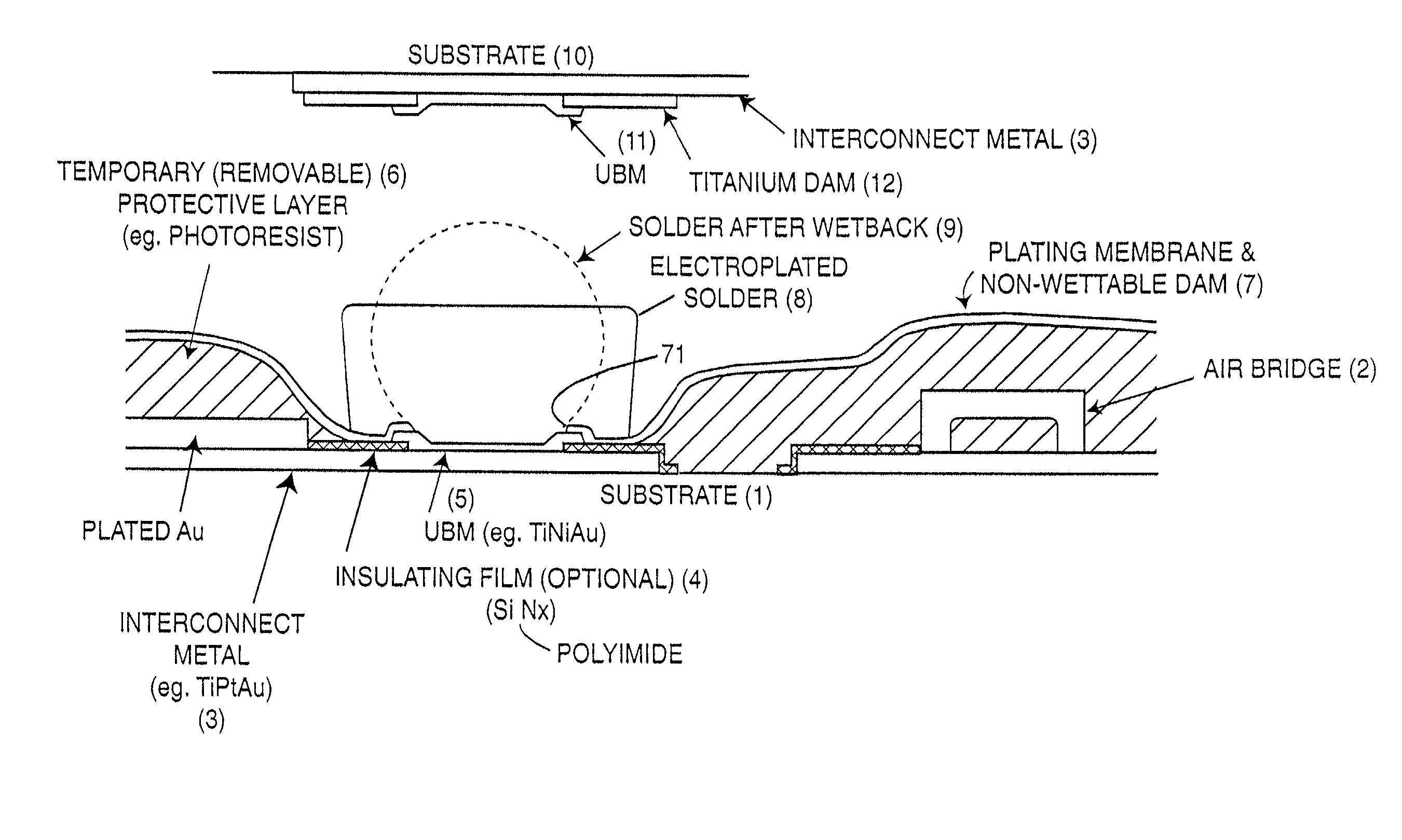
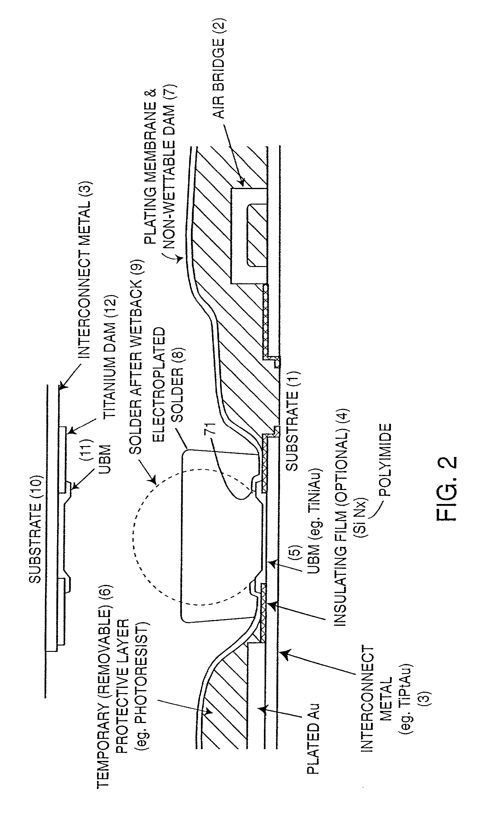
[0025] The preferred solder bump structure of this invention is illustrated in FIGS. 2, 2(a), and 3. The structure is formed on a substrate 1 that contains either group IV or group III-V semiconductor devices and circuits. The devices and circuits may contain exposed air bridges 2, microelectromechanical elements such as MEMS switches (not shown), and / or optoelectronic devices with exposed optical surfaces and coatings (not shown, either). These devices and circuits typically utilize exposed gold and / or titanium and / or platinum interconnect lines 3. The solder bump defining structure is a multilayer structure. The first layer is preferably an optional patterned insulating film 4 or a sealant feature on top of which the underbump metallization UBM 5 is applied followed by a patterned layer of a photoresist 6 and, finally, by a thin layer 7 of a metal, preferably, titanium.
[0026] Preferably the interconnect 3 is at least partially covered by an insul...
PUM
| Property | Measurement | Unit |
|---|---|---|
| thickness | aaaaa | aaaaa |
| thickness | aaaaa | aaaaa |
| thickness | aaaaa | aaaaa |
Abstract
Description
Claims
Application Information