

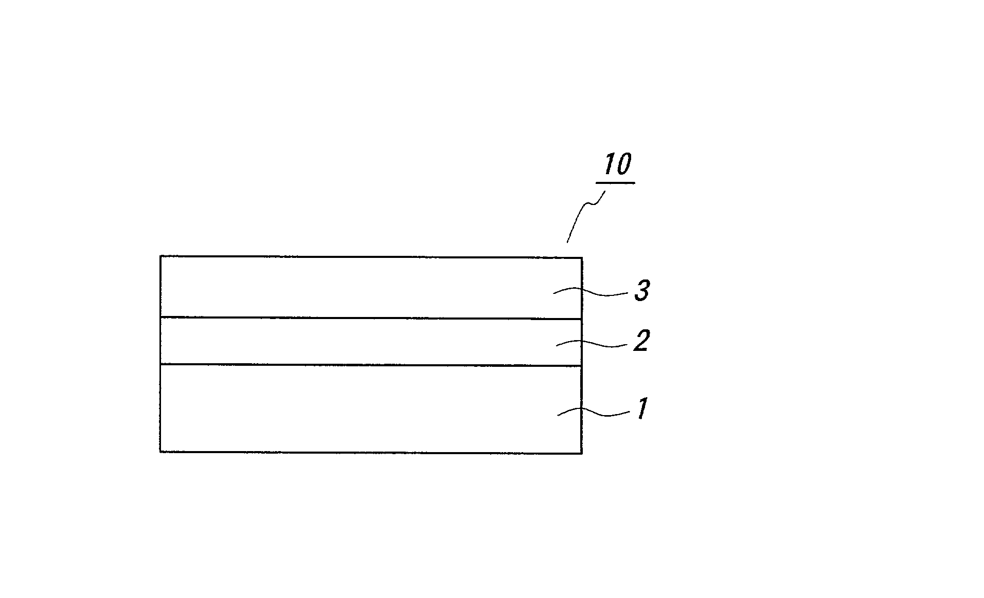
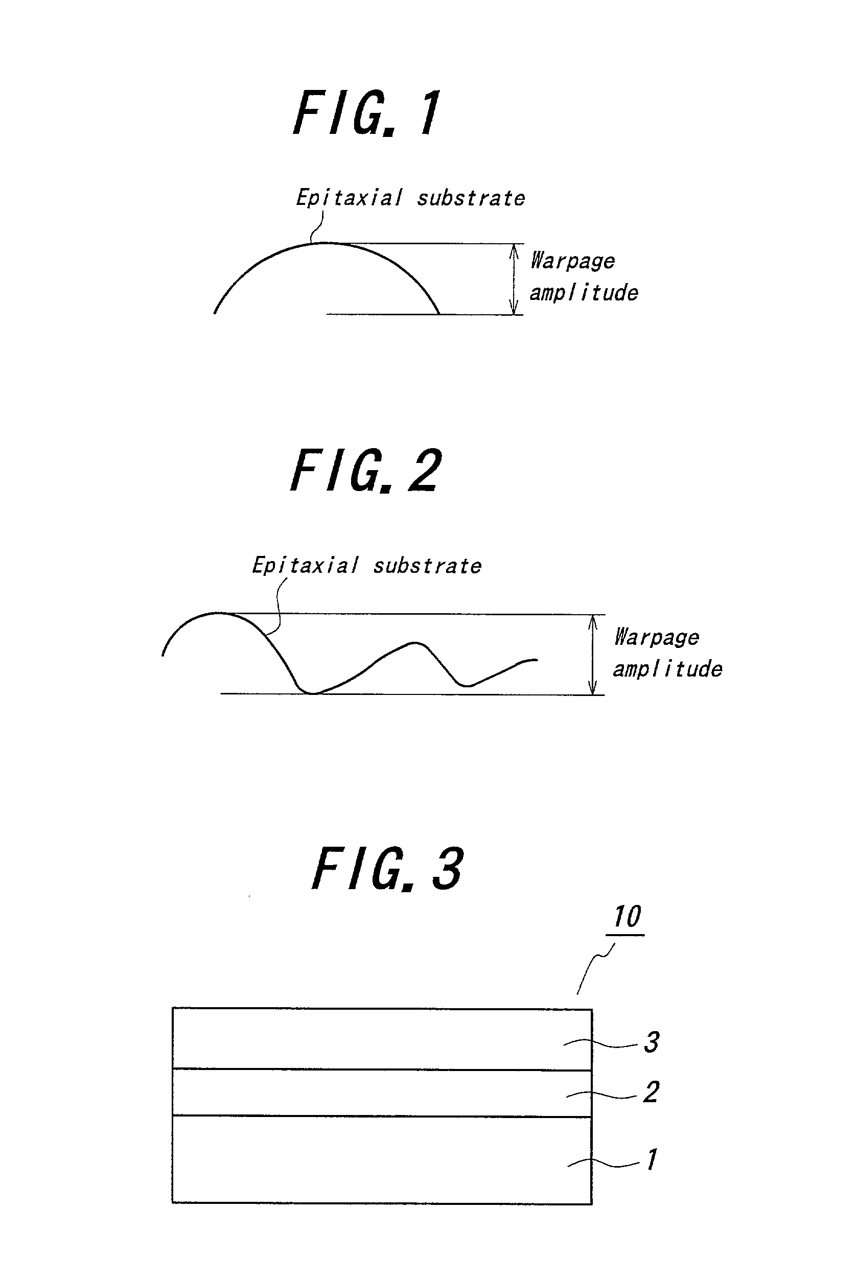
Epitaxial base substrate and epitaxial substrate
a technology of epitaxial substrate and epitaxial substrate, which is applied in the direction of crystal growth process, polycrystalline material growth, semiconductor/solid-state device details, etc., can solve the problems of deteriorating semiconductor element manufacturing yield ratio, uneven thickness of epitaxial substrate, and large warping of epitaxial substra
- Summary
- Abstract
- Description
- Claims
- Application Information
AI Technical Summary
Benefits of technology
Problems solved by technology
Method used
Image

Examples
example
[0048] A substrate made of c-faced sapphire single crystal was employed, and then, set on a susceptor installed in a reactor. A TMA and an NH.sub.3 were used as an Al raw material gas and an N raw material gas, respectively. Then, the TMA and the NH.sub.3 were introduced into the reactor and supplied onto the substrate, on the condition of the (V raw material gas / III raw material gas) flow rate ratio of 450 and the forming pressure of 15 Torr. Thereafter, the substrate was heated to 1200.degree. C., and an AlN film as a buffer film was formed in a thickness of 1 .mu.m on the substrate.
[0049] The full width at half maximum in X-ray rocking curve at (0002) reflection was 60 seconds, and the good crystal quality of the AlN film was confirmed. The surface roughness Ra was 2.ANG., and the good flatness of the AlN film was also confirmed. Moreover, the screw-type dislocation density of the AlN film was 1.times.10.sup.7 / cm.sup.2.
[0050] Thereafter, the forming pressure was varied to atmosph...
PUM
| Property | Measurement | Unit |
|---|---|---|
| temperature | aaaaa | aaaaa |
| temperature | aaaaa | aaaaa |
| temperature | aaaaa | aaaaa |
Abstract
Description
Claims
Application Information