Atmospheric pressure plasma enhanced abatement of semiconductor process effluent species

a technology of atmospheric pressure and plasma, applied in the field of plasma generation, can solve the problems of limited thermal destruction efficiency, high temperature required to decompose some materials, and the impact of the semiconductor industry

Inactive Publication Date: 2002-08-15
APPLIED MATERIALS INC
View PDF0 Cites 20 Cited by
  • Summary
  • Abstract
  • Description
  • Claims
  • Application Information

AI Technical Summary

Problems solved by technology

The semiconductor industry is one of the many industries particularly affected because the fabrication of computer chips involves toxic chemicals, e.g., arsine, phosphine, and chlorine.
However, the efficiency of thermal destruction is limited by the thermal stability of the effluent species.
The high temperatures required to decompose some materials can only be achieved by using electric furnaces or reactant gases that release energy via exothermic reactions.
Both methods use a significant amount of resources leading to high costs of ownership.
Furthermore, when certain chloride compounds are exposed to high temperatures in the presence of oxygen, they can react to form extremely hazardous polychlorinated compounds.
Additionally, the high temperatures reached in thermal furnaces result in a significant increase in the degradation rate of materials of construction leading to a shorter lifetime of the abatement units.
Traditional dry and wet scrubbing techniques are limited in their ability to destroy certain effluent compounds such as organic chlorides.
Additionally, dry scrubbing methods use vessels containing beds of adsorbent material whose surface physically adsorbs the molecules of the effluent species being abated, but such methods produce a vessel of hazardous material for disposal.
Likewise, wet scrubbing techniques produce large quantities of contaminated fluids that must be disposed as toxic waste thereby increasing the cost of the abatement system and associated semiconductor manufacturing facility.
However, placement of these non-thermal plasma systems between the processing chamber and the vacuum pump, can present problems such as deposit formation, viz., the precipitation of solids in the vacuum pump, which causes clogging of the exhaust lines leaving the vacuum pump.
Additionally, the positioning of the plasma abatement system near the processing chamber may adversely affect the semiconductor tool and processing.

Method used


Image

  • Atmospheric pressure plasma enhanced abatement of semiconductor process effluent species
  • Atmospheric pressure plasma enhanced abatement of semiconductor process effluent species
  • Atmospheric pressure plasma enhanced abatement of semiconductor process effluent species

Examples


Embodiment Construction

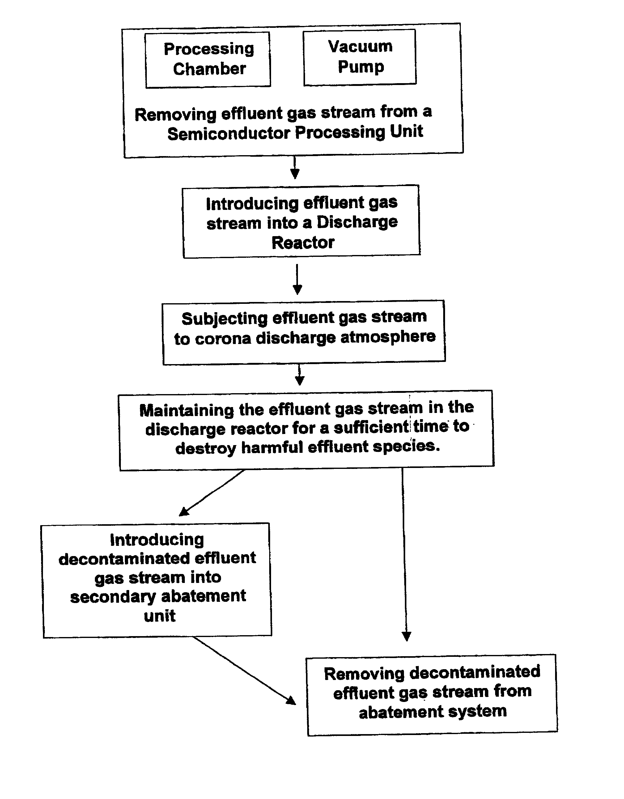
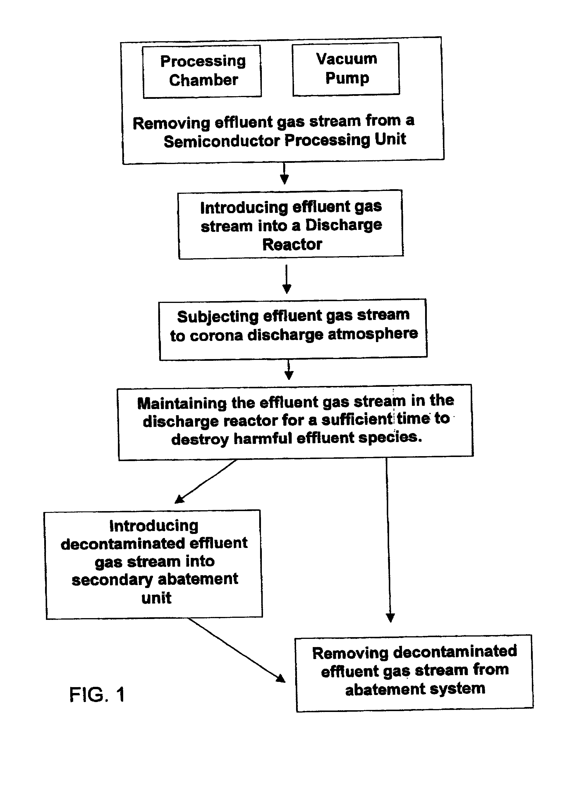
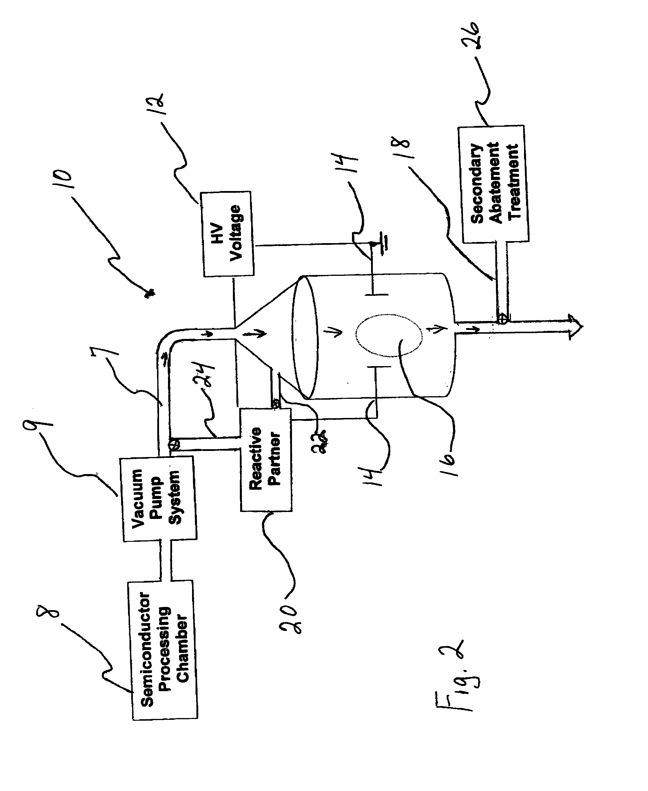
[0030] The present invention is based on the discovery that considerable benefit may be obtained by positioning a discharge reactor, maintained at approximately atmospheric pressure, after the processing chamber and vacuum pump system in the semiconductor processing unit. In particular it has been found that formation of unwanted precipitating deposits is greatly reduced thereby, essentially eliminating blockage formation in the vacuum pump and / or exhaust lines leaving the vacuum pump. Additionally, placement of the plasma abatement system after the vacuum system and away from the semiconductor processing chamber reduces interference with the processing tool.

[0031] The present invention provides for methods and systems for non-thermal plasma abatement of harmful unused semiconductor processing gases and reactive products formed in a semiconductor processing chamber. The plasma abatement involves using a plasma source to convert toxic or environmentally harmful emissions into harmles...


PUM

PropertyMeasurementUnit
voltageaaaaaaaaaa
voltagesaaaaaaaaaa
voltagesaaaaaaaaaa

Abstract

The present invention relates to a method and system for non-thermal abatement of effluent species generated in a semiconductor processing unit. In the method, an effluent stream is introduced into a discharge reactor wherein the components of the effluent stream are subjected to a corona discharge and maintained therein for a sufficient time to detoxify and / or dissociate the harmful components of the effluent stream. The discharge reactor, maintained at approximately atmospheric pressure, is positioned after the low-pressure semiconductor processing chamber and connecting vacuum pump system to limit interference with the semiconductor plasma processing tool.

Description

[0001] 1. Field of the Invention[0002] The present invention relates generally to plasma generation and more specifically to plasma abatement methods and systems for treatment of waste emissions from a semiconductor processing chamber.[0003] 2. Description of the Related Art[0004] Release of gases that are toxic to humans or generally harmful to the global environment, is of growing concern to industrial producers of such emissions. The semiconductor industry is one of the many industries particularly affected because the fabrication of computer chips involves toxic chemicals, e.g., arsine, phosphine, and chlorine. Other very stable compounds are also generated in semiconductor manufacturing processes that are capable of reaching the upper atmosphere and inflicting serious and long-term damage to the planetary climate. Consequently, governments worldwide are taking a more aggressive role in legislating and regulating the amount of air pollution generated by the semiconductor industr...

Claims


Application Information

Patent Timeline
Patent Type & Authority Applications(United States)
IPC IPC(8): B01D53/32
CPCB01D53/32Y10S438/905
Inventor ARNO, JOSE I.
Owner APPLIED MATERIALS INC
Why Eureka
Try Eureka