Semiconductor memory apparatus using tunnel magnetic resistance elements

Inactive Publication Date: 2002-09-12
NEC CORP
View PDF3 Cites 71 Cited by
  • Summary
  • Abstract
  • Description
  • Claims
  • Application Information

AI Technical Summary

Benefits of technology

0012] An object of the present invention is to provide an MRAM that needs not a process for form

Problems solved by technology

Thus, the production cost rises.
Thus, the structure of a switch for selecting the vo

Method used


Image

  • Semiconductor memory apparatus using tunnel magnetic resistance elements
  • Semiconductor memory apparatus using tunnel magnetic resistance elements
  • Semiconductor memory apparatus using tunnel magnetic resistance elements

Examples


Embodiment Construction

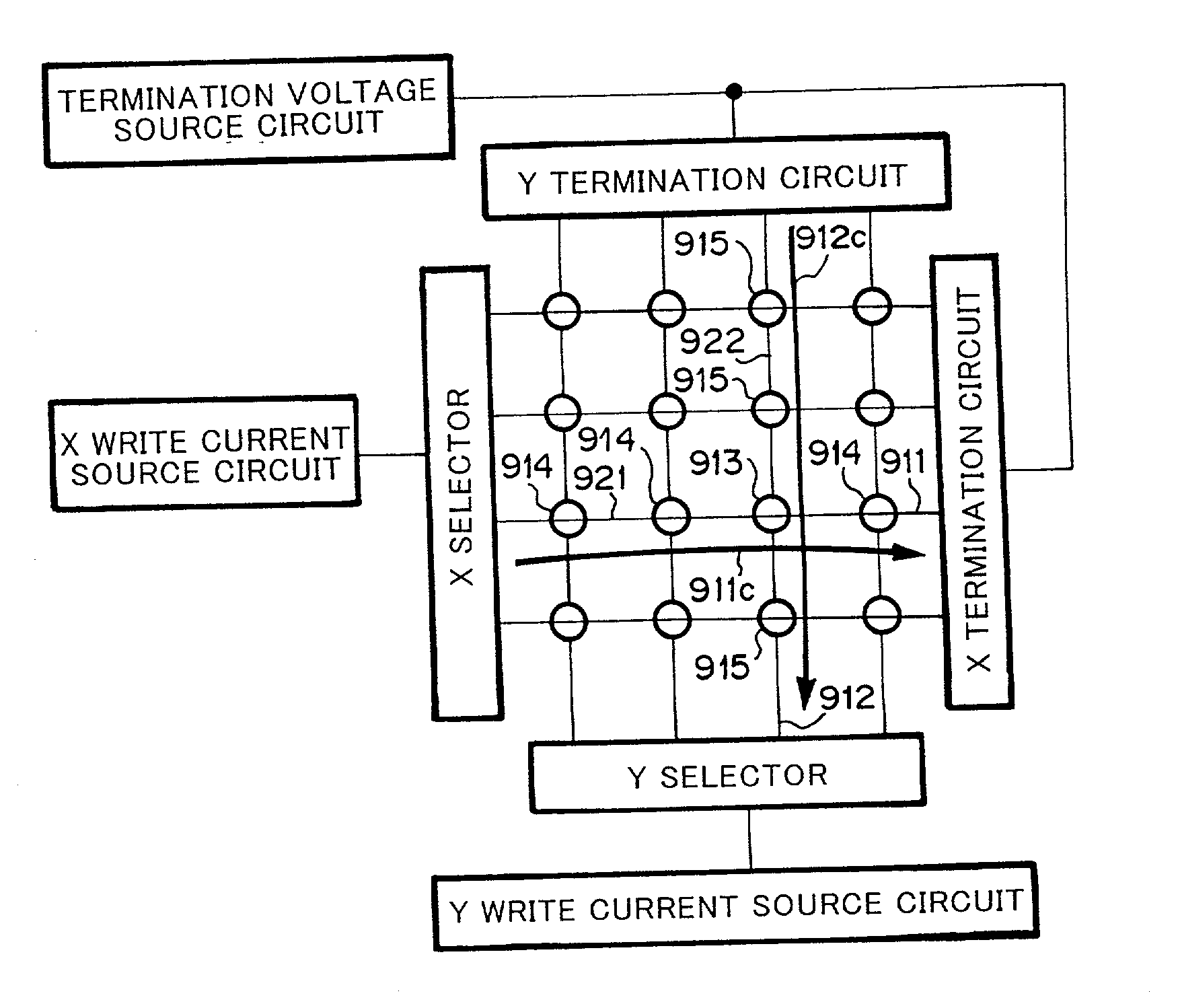
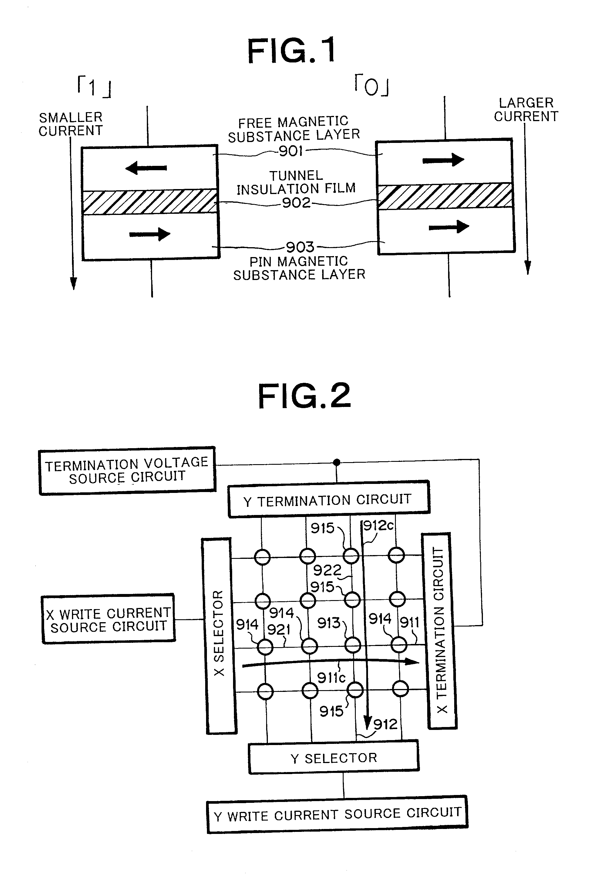
[0068] FIG. 6 is a schematic diagram showing the concept of an MRAM according to an embodiment of the present invention. FIG. 6 shows only one cell array and one sense amplifier. According to the embodiment of the present invention, a selected word line 102 connected to a selected cell 101 is connected to a read power source 104. A selected bit line 103 connected to the selected cell 101 is connected to an input of a sense amplifier 105. The voltage of the selected bit line is determined by an input circuit of the sense amplifier 105. In the example shown in FIG. 6, the voltage of the read power source 104 is 1.4 V, whereas the input voltage of the sense amplifier is 1.1 V. Thus, their voltages are different. Because switches connected to non-selected word lines 106 other than the selected word line 102 and switches connected to non-selected bit lines 107 other than the selected bit line 103 are caused to be in a high impedance state, the non-selected word lines 106 and the non-sele...


PUM


Abstract

A semiconductor memory apparatus using tunnel magnetic resistance elements comprises a plurality of cell arrays. When data is read from a cell in one of the cell array, a word line connected to the cell is connected to a voltage source, a bit line connected to the cell is connected to an input of a sense amplifier, word lines in the cell array concerned except for the word line connected to the cell and bit lines in the cell array concerned except for the bit line connected to the cell are isolated. A subtracter subtracts an offset current which is generated in another cell array from a current flowing from the bit line connected the cell. An integrator integrates the result of the subtraction. A comparator, a read current value register, and a reference value register performs self-reference reading method on the result of the integration.

Description

BACKGROUND OF THE INVENTION[0001] 1. Field of the Invention[0002] The present invention relates to a semiconductor memory apparatus using tunnel magnetic resistance elements as memory cells. Hereinafter, the tunnel magnetic resistance element is referred to as TMR element or simply cell. In addition, the semiconductor memory apparatus using the TMR elements is referred to as MRAM.[0003] 2. Description of the Prior Art[0004] FIG. 1 shows the theory of an TMR element. The TMR element is composed of a free magnetic substance layer 901, a tunnel insulation film 902, and a pin magnetic substance layer 903 that are successively disposed. The amount of a current that flows in the tunnel insulation film 902 varies depending on the orientation of the magnetization of the free magnetic substance layer 901. A larger current or a smaller current is assigned "1" whereas the other current is assigned "0". The orientation of the pin magnetic substance layer 903 has been fixed from the time the dev...

Claims


Application Information

Patent Timeline
IPC IPC(8): G11C11/15G11C11/14G11C11/16H01L21/8246H01L27/10H01L27/105H01L43/08
CPCG11C11/16G11C11/1673G11C11/1675
Inventor SUGIBAYASHI, TADAHIKOSAKIMURA, NOBORUHONDA, TAKESHI
Owner NEC CORP
Why Eureka
Try Eureka