Semiconductor light-emitting device

a technology of semiconductors and light-emitting devices, which is applied in the manufacture of semiconductor/solid-state devices, semiconductor devices, electrical devices, etc., can solve the problems of difficult control of epitaxial growth of crystals, low reliability, and high power for operation, and achieves the reduction of the amount of substances applied to the light extraction section, the effect of reducing the diameter of the light extraction section and high emission directivity

Inactive Publication Date: 2002-09-26
SHOWA DENKO KK
View PDF13 Cites 24 Cited by
  • Summary
  • Abstract
  • Description
  • Claims
  • Application Information

AI Technical Summary

Benefits of technology

0071] Like a conventional semiconductor light-emitting device, the semiconductor light-emitting device of the present invention may be encapsulated with a resin. A resin used for encapsulation preferably contains any one species selected from among epoxy resins, urea resins, and silicone resins, which resins transmit light emitted from the semiconductor light-emitting device. A light-shielding function may be imparted to the resin used for encapsulation (encapsulation resin). In this case, the encapsulation resin may be mixed with a light-shielding substance, but application of the substance to a light extraction section is prevented. The amount of the substance applied to the light extraction section may be reduced.
0072] The semiconductor light-emitting device of the present invention exhibits high emission directivity; enables reduction in the diameter of a light extraction section; has a small size and high reliability; and exhibits high emission output. Therefore, the device can be used in the form of a conventional semiconductor light-emitting device or a resin-encapsulated semiconductor light-emitting device. The semiconductor light-emitting device is suitably used in fields in which a laser diode or a current-constricting semiconductor light-emitting device is used, in addition to fields in which a conventional semiconductor light-emitting device is used. In addition, particularly, the device is suitably used in a variety of optical sensors which are mainly used for detecting the displacement or the position of a body, or is used as a light extraction section of an optical communication apparatus, such as a light source for IR-ray communication or optical fiber.
0073] The semiconductor light-emitting device of the present invention has advantages in emission directivity, high emission output, high reliability, and low production cost, which advantages cannot be obtained in a conventional semiconductor light-emitting device, a laser diode, or a current-constricting semiconductor light-emitting device. Therefore, when the semiconductor light-emitting device is used in an apparatus, the apparatus can attain high reliability, low production cost, miniaturization, and power savings.

Problems solved by technology

However, a laser diode involves disadvantages, in that it is expensive and requires high power for operation thereof, and thus LEDs exhibiting emission directivity have been proposed.
However, a current-constricting LED involves disadvantages, including difficulty in control of epitaxial growth of crystal and low reliability attributed to flow of high current to a portion of the crystal.
In addition, although a current-constricting LED is less expensive than a laser diode, the LED has a complicated structure and is expensive as compared with a conventional LED.
However, when a reflection plate or a reflection cup is provided or formed, the resultant light-emitting apparatus may be expensive, and miniaturization of the apparatus is difficult, which is unsatisfactory.
In addition, a light emission region cannot be formed as small as that of a laser diode or a current-constricting LED, and thus such a conventional LED is difficult to use as a point-source light.
However, light which leaks from the side of the LED becomes stray light, and thus noise increases and S / N ratio decreases.

Method used


Image

  • Semiconductor light-emitting device
  • Semiconductor light-emitting device
  • Semiconductor light-emitting device

Examples


examples 1 through 10

[0075] The semiconductor light-emitting device of the present invention was produced by use of an epitaxial wafer for producing a visible-light-emitting device (emission wavelength: 660 nm). The epitaxial wafer was produced as follows. On a p-type GaAs substrate, a p-type Ga.sub.1-x1Al.sub.x1As (0.5

[0076] At The p-type transparent substrate layer and the n-type layer of the wafer were subjected to deposition and alloying of an Au alloy, to thereby form ohmic electrodes. On the electrode which was formed on the n-type layer, openings of 120 .mu.m.phi. were formed at an interval of 350 .m...

example 11

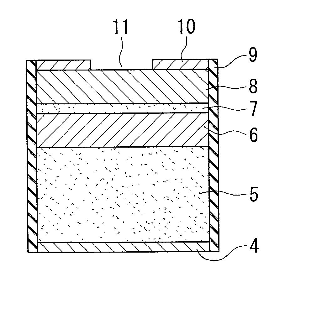
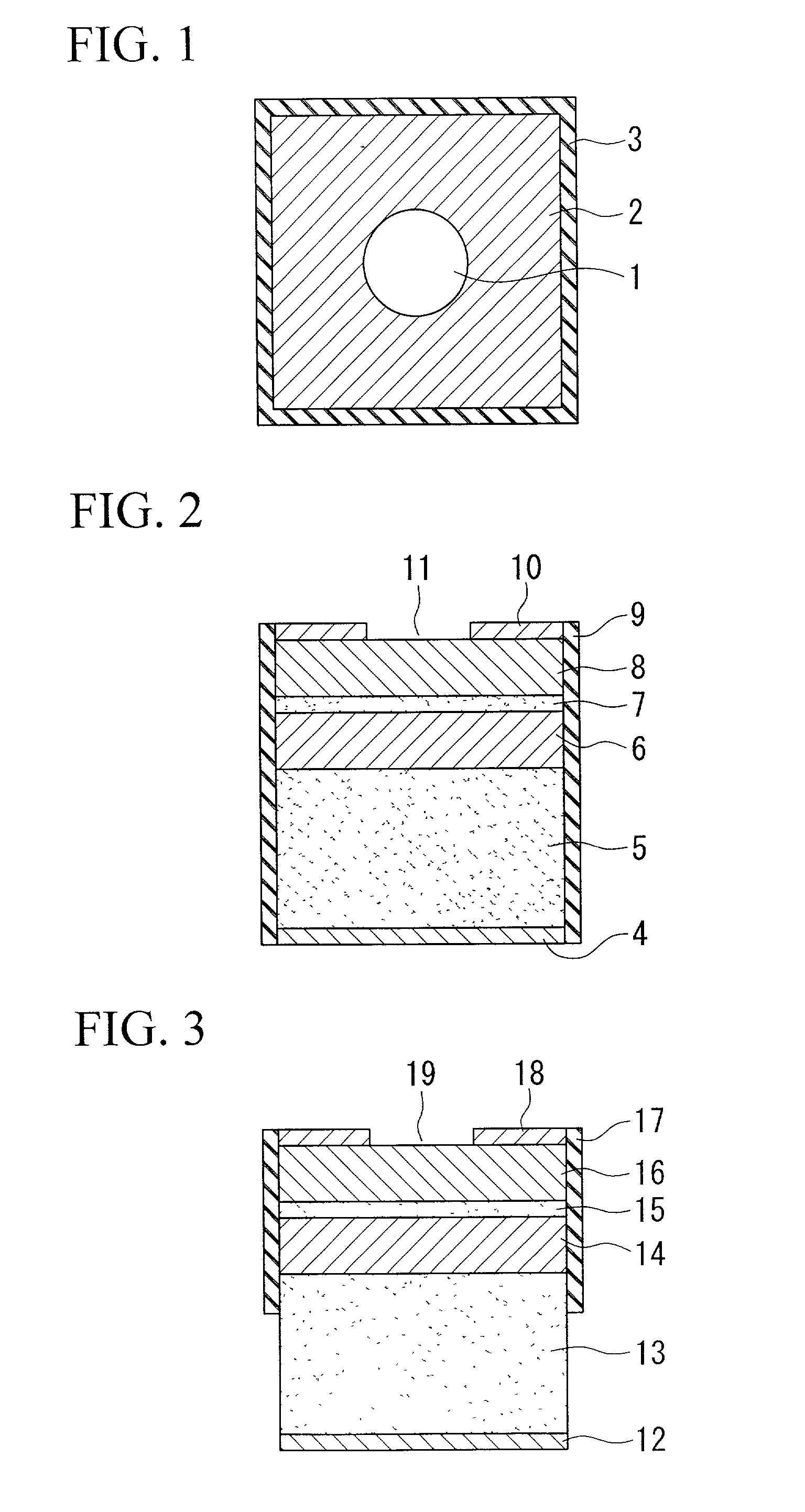
[0082] FIG. 3 shows a cross-sectional view of the semiconductor light-emitting device produced in Example 11. An epitaxial wafer for the semiconductor light-emitting device was produced as follows. On a Zn-doped p-type GaAs single-crystal substrate 13 (thickness: 250 .mu.m), through a liquid epitaxial method, a Zn-doped p-type GaAlAs cladding layer 14 (thickness: 20 .mu.m), a Zn-doped GaAlAs active layer 15 (thickness: about 1 .mu.m), and a Te-doped n-type GaAlAs cladding layer 16 (thickness: 30 .mu.m) were grown successively. In the active layer, the proportions of Ga, Al, and As were regulated to 0.65:0.35:1, so as to attain an emission wavelength of 660 nm. In the p-type cladding layer 14 and the n-type cladding layer 16, the proportions of Ga, Al, and As were regulated to 0.35:0.65:1, so as to transmit light of 660 nm. In the semiconductor light-emitting device produced from the wafer, the GaAs substrate 13 absorbs light of 660 nm, and thus light is not emitted from the surface ...

example 12

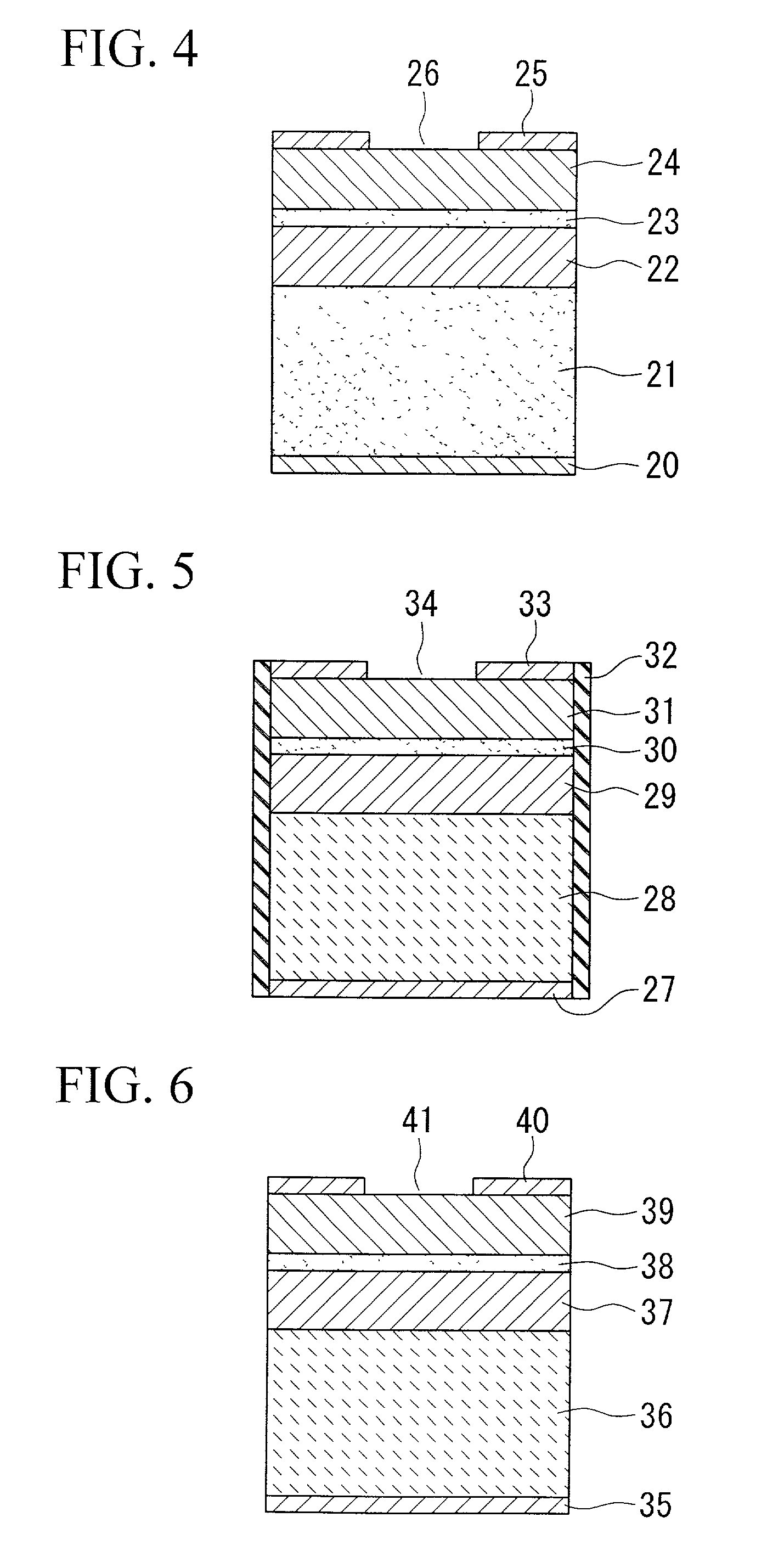
[0087] FIG. 5 shows a cross-sectional view of the semiconductor light-emitting device produced in Example 12. In this Example, an epitaxial wafer was produced as follows. On a Zn-doped p-type GaAs single-crystal substrate (thickness: 250 .mu.m), through a liquid epitaxial method, a Zn-doped p-type GaAlAs transparent substrate layer 28 (thickness: 100 .mu.m), a Zn-doped GaAlAs p-type cladding layer 29 (thickness: 20 .mu.m), a Zn-doped GaAlAs active layer 30 (thickness: about 1 .mu.m), and a Te-doped n-type GaAlAs cladding layer 31 (thickness: 30 .mu.m) were grown successively. In the active layer, the proportions of Ga, Al, and As were regulated to 0.65:0.35:1, so as to attain an emission wavelength of 660 nm. In the p-type transparent substrate, and the p-type and n-type cladding layers, the proportions of Ga, Al, and As were regulated to 0.35:0.65:1, so as to transmit light of 660 nm. Subsequently, the GaAs substrate was removed through etching, to thereby form the epitaxial wafer ...


PUM

PropertyMeasurementUnit
thicknessaaaaaaaaaa
particle sizeaaaaaaaaaa
lengthaaaaaaaaaa

Abstract

A small-sized semiconductor light-emitting device of high emission directivity and high output is provided. A portion of a light extraction section of a semiconductor light-emitting device including a pn-junction portion is covered with a light-shielding substance of low conductivity. The electrical resistance of the light-shielding substance is 106 OMEGAm or higher, and the substance contains powder of at least one species selected from metals and pigments. The powder of metal contains at least one species selected from among Al, Cu, Ag, Au, Pt, Ti, Ni, Sn, Pb, Mg, Zn, Fe, Co, and Cr. The powder is a plate-like powder having a thickness falling within a range of 0.001-10 mum and a length falling within a range of 0.01-100 mum.

Description

[0001] This application claims the benefit pursuant to 35 U.S.C. .sctn.119(e)(1) of U.S. Provisional Applications, No. 60 / 217,105 filed Jul. 10, 2000, No. 60 / 263,241 filed Jan. 23, 2001, and No. 60 / 267,423 filed Feb. 9, 2001.[0002] The present invention relates to a semiconductor light-emitting device, and more particularly to a semiconductor light-emitting device exhibiting enhanced emission directivity.[0003] Light-emitting diodes (hereinafter referred to as "LEDs") and laser diodes are known as light-emitting devices including semiconductors. For example, an LED including a Group III-V compound semiconductor is produced through epitaxial growth of a layer of GaP, GaAsP, GaAs, GaAlAs, GaAlInP, or GaN on a single-crystal substrate of GaP or GaAs. The LED includes pn-junction portions which are formed of one or more p-type layers and one or more n-type layers, and has an appropriate structure such that light is emitted when electrons are introduced into the pn-junction portions.[000...

Claims


Application Information

Patent Timeline
Patent Type & Authority Applications(United States)
IPC IPC(8): H01L33/46
CPCH01L33/46
Inventor KAMEMURA, TAKAYUKIMITANI, KAZUHIROKOBAYASHI, TERUYUKIUOTANI, NOBUONAKAMURA, KASUMIITOH, YUJI
Owner SHOWA DENKO KK
Why Eureka
Try Eureka