Magnetic random-access memory

a random access and memory technology, applied in the field of magnetic random access memory, can solve the problems of difficult to reduce the area of each cell, complicated manufacturing process, etc., and achieve the effect of increasing the degree of freedom in the design of device pattern and higher integration level

Inactive Publication Date: 2002-10-03
RENESAS ELECTRONICS CORP
View PDF0 Cites 35 Cited by
  • Summary
  • Abstract
  • Description
  • Claims
  • Application Information

AI Technical Summary

Benefits of technology

0031] This serves to increase the degree of freedom in device pattern design a

Problems solved by technology

The structure of memory cells which is perpendicular to the plane of the substrate 150 is so complex tha

Method used


Image

  • Magnetic random-access memory
  • Magnetic random-access memory
  • Magnetic random-access memory

Examples


first embodiment

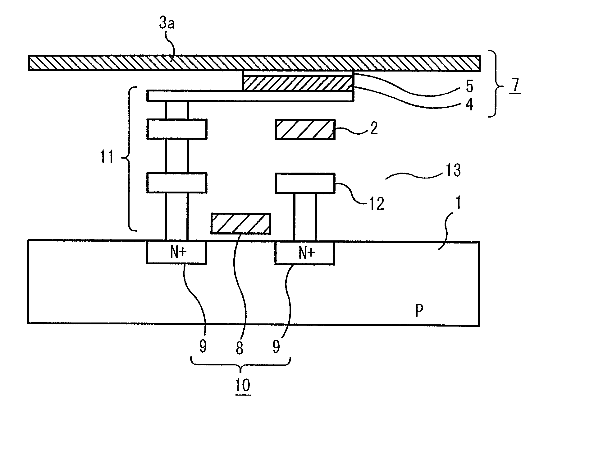
[0050] FIG. 1 is a cross-sectional diagram showing the construction of an MRAM device according to a first embodiment of the invention.

[0051] Referring to FIG. 1, the MRAM device comprises a p-type semiconductor substrate 1 (hereinafter referred to simply as the substrate 1), on which parallel write word lines 2 serving as first word lines and parallel bit lines 3a are arranged at specific intervals, the write word lines 2 and the bit lines 3a intersecting one another. A free-spin layer 4 serving as a first magnetic substance layer and a thin insulator layer 5 stacked on top of the free-spin layer 4 are located in each area of intersection of the write word lines 2 and the bit lines 3a. The bit lines 3a are made of ferromagnetic metal, such as cobalt, nickel or iron. The direction of electron spin in the individual bit lines 3a is fixed to the direction of their length by previously subjecting them to a strong magnetic field or applying other form of treatment. TMR elements 7 are fo...

second embodiment

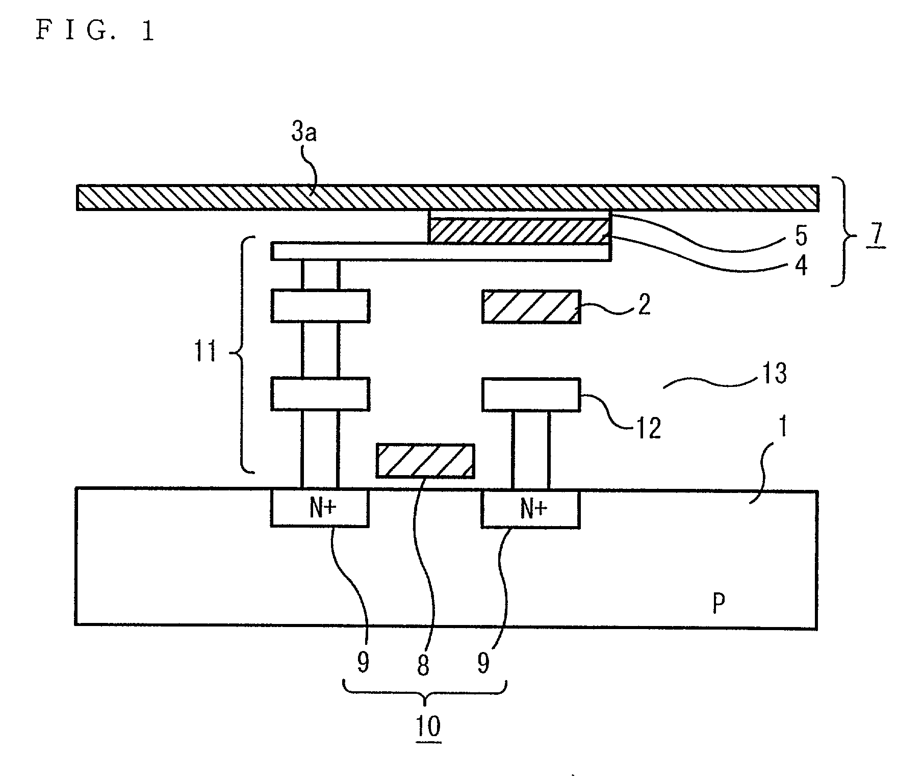
[0058] While the aforementioned first embodiment requires the separately formed write word lines 2 and readout word lines 8, an MRAM device of a second embodiment employs word lines which are used for performing both data read and write operations.

[0059] Referring to FIG. 3, the MRAM device has common word lines 8a which perform the read and write operations and serve as gate electrodes of individual access transistors 10. TMR elements 7 are arranged at individual intersections of bit lines 3 formed in an upper layer and the common word lines 8a, each TMR element 7 having a sandwich structure comprising a fixed-spin layer 6 serving as a second magnetic substance layer, an insulator layer 5 and a free-spin layer 4 from top to bottom. Designated by the numeral 14 is a contact hole used for connecting the free-spin layer 4 to one of source / drain regions 9.

[0060] In this example, a dedicated magnetic substance layer in which the spin direction is fixed to the bit line direction is used ...

third embodiment

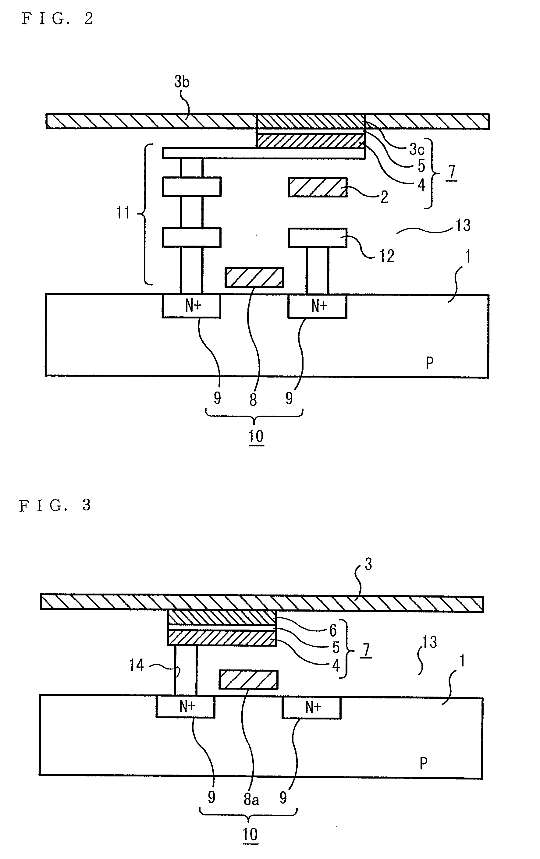
[0069] While the aforementioned second embodiment employs the common word lines 8a which perform both the data read and write operations, it might be impossible to implement this kind of common word lines 8a combining the functions of the write word lines 2 and the readout word lines 8 in modern hybrid design in which the MRAM device is integrated with a multilayer interconnection logic device, for instance. Since interconnection layers are stacked so higher than the substrate 1 in the modern multilayer interconnection logic device, there is no alternative but to form the TMR element 7 at a position much higher than the readout word line 8 of the access transistor 10, making it impossible to combine the write word line 2 and the readout word line 8 into a common word line.

[0070] FIG. 7 shows the construction of an MRAM device according to a third embodiment of the invention, in which a write word line 2 and a readout word line 8 are electrically connected to each other to set them a...


PUM


Abstract

A magnetic random-access memory comprises a semiconductor substrate (1) on which write word lines (2) and bit lines (3) intersecting each other are arranged, TMR elements (7) formed individually in areas of intersection of the write word lines (2) and the bit lines (3), each TMR element (7) being formed by stacking a free-spin layer (4) whose magnetization direction is variable, a fixed-spin layer (6) whose magnetization direction is fixed and an insulator layer (5) placed between the first and second magnetic substance layers, and access transistors (10). The TMR elements (7) are located where word lines (8a) which serve as gates of the access transistors (10) intersect the bit lines (3) so that the word lines (8a) perform the functions of both write and read word lines. This arrangement reduces the complexity involved in creating a multilayer interconnection structure, simplifies the structure and manufacturing processes of the magnetic random-access memory, and enables its miniaturization and a higher level of integration.

Description

BACKGROUND OF THE INVENTION AND RELATED ART STATEMENT[0001] The present invention relates to a magnetic random-access memory (MRAM) having a magnetic substance structure.[0002] An MRAM is a memory device which utilizes a phenomenon that the resistance to an electric current flowing through a magnetic substance structure varies depending on the direction of electron spin (magnetization direction) in the magnetic substance. A tunneling magnetoresistive (TMR) element is an example of an element conventionally used for performing information storage operation. Each cell of a magnetic memory, capable of storing one bit of information, is made of one each TMR element and metal-oxide-semiconductor (MOS) transistor.[0003] FIG. 16 is a cross-sectional diagram showing the construction of a conventional MRAM device. In this Figure, designated by the numeral 100 is a TMR element having a sandwich structure with a thin insulator layer 102 sandwiched between a first magnetic substance layer 101 a...

Claims


Application Information

Patent Timeline
IPC IPC(8): G11C11/15G11C11/14G11C11/16H01L21/8246H01L27/105H01L27/22H01L43/08
CPCB82Y10/00H01L27/228H01L27/224G11C11/16H10B61/10H10B61/22
Inventor KOMORI, SHIGEKI
Owner RENESAS ELECTRONICS CORP
Why Eureka
Try Eureka