Method for forming copper lines for semiconductor devices

a technology for semiconductor devices and copper lines, which is applied in the manufacturing of semiconductor/solid-state devices, basic electric elements, electric devices, etc., can solve the problems of difficult etching of copper, inconvenient use of aluminum in giga-bit level drams, and conventional method for forming copper lines in semiconductor devices, so as to prevent misalignment and dishing, and stable electrical properties

Inactive Publication Date: 2002-10-03
SK HYNIX INC
View PDF0 Cites 16 Cited by
  • Summary
  • Abstract
  • Description
  • Claims
  • Application Information

AI Technical Summary

Benefits of technology

0019] Accordingly, it is an object of the present invention to provide a method for forming a copper line for a semiconductor device with stable electrical properties by utilizing the difference in polishing rate between the self aligned tungsten film pattern corresponding to predetermined copper line regions and the copper film wherein the tungsten film pattern serves as a hard mask to prevent misalignment and dishing during CMP process.

Problems solved by technology

However, aluminum is not suitable for use in giga-bit level DRAMs due to its relatively high resistance and limitation in reducing the fine line widths necessary for extremely high density devices.
However, it is difficult to etch copper.
As described above, the conventional method for forming a copper line in a semiconductor device has a disadvantage in that the dishing phenomenon occurs on the copper line formed in the trench due to a polishing rate difference between the copper film and the Ti / TiN film.
The recessed areas of the copper lines disrupts the desired planarity of the wafer surface and complicates subsequent processing steps.
In addition, the electrical properties of the copper line are degraded, and a process yield and reliability of the resulting devices are reduced.

Method used


Image

  • Method for forming copper lines for semiconductor devices
  • Method for forming copper lines for semiconductor devices
  • Method for forming copper lines for semiconductor devices

Examples


Embodiment Construction

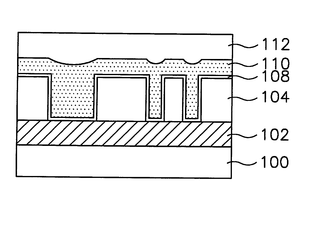
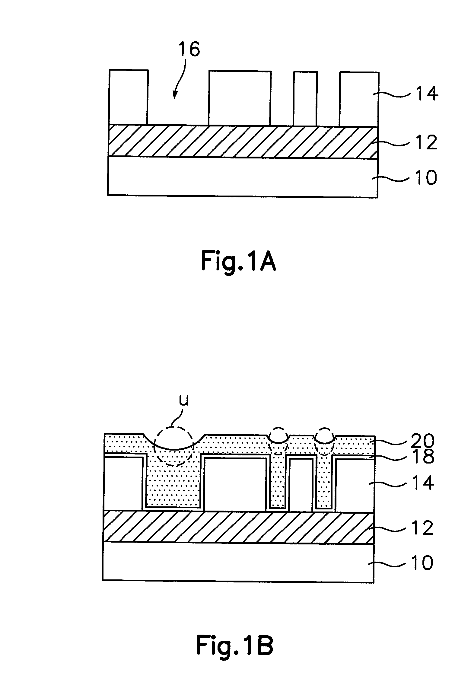
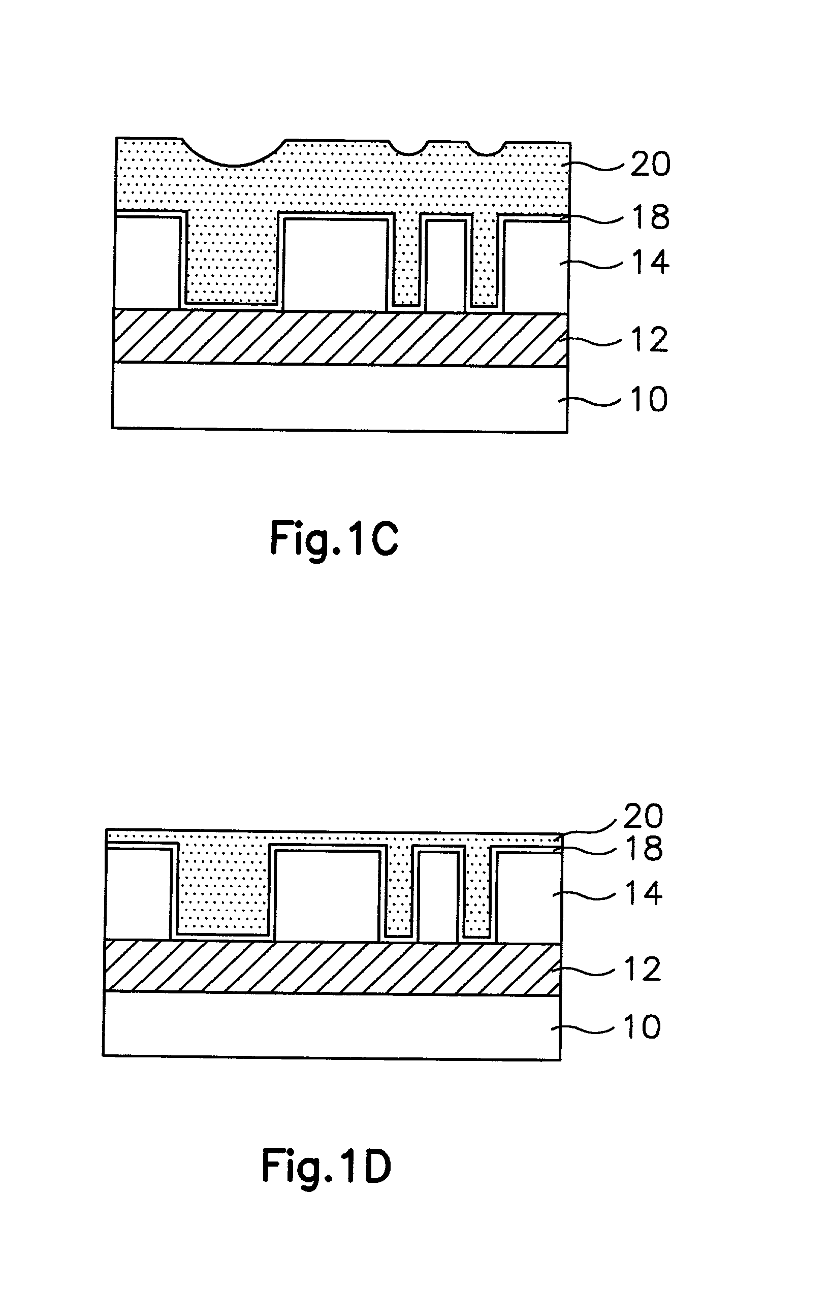
[0024] A method for forming a copper line of a semiconductor device in accordance with the present invention will now be described in detail with reference to the accompanying drawings.

[0025] A substructure consisting of a word line, bit line and capacitor is first formed on a semiconductor substrate 100 and a first interlayer insulating film 102 is then formed on the resulting structure.

[0026] A metal line contact plug (not shown) is then formed through first interlayer insulating film 102 to make contact to a predetermined metal line contact region of the substrate and a second interlayer insulating film 104 is then formed over the resulting structure.

[0027] Thereafter, a trench 106 exposing a predetermined metal line region and a metal line contact plug (not shown) is formed by etching the second interlayer insulating film 104 (see FIG. 2A).

[0028] A diffusion barrier film 108, preferably a Ti / TiN film, is then formed over the resulting structure.

[0029] A copper film 110 is then d...


PUM

PropertyMeasurementUnit
insulatingaaaaaaaaaa
semiconductoraaaaaaaaaa
electrical propertiesaaaaaaaaaa

Abstract

The present invention discloses a method for forming a copper line of a semiconductor device by using a new damascene process. A copper film is formed over and into trenches formed in a lower insulating layer, a tungsten film is formed on the copper film and planarized, a self-aligned tungsten film pattern is formed over the predetermined copper line region by etching the tungsten film, and a chemical mechanical polishing method is performed using the tungsten film pattern as a hard mask. As a result, the copper line having a generally planar surface and stable conductivity is formed by preventing a misalignment and dishing phenomena, thereby improving device performance, reliability, and process yield.

Description

BACKGROUND OF THE INVENTION[0001] This application relies for priority upon Korean Patent Application No. 2001-16941 filed on Mar. 30, 2001, the contents of which are herein incorporated by reference in their entirety.[0002] 1. Field of the Invention[0003] The present invention relates to a method for forming a copper lines in a semiconductor device and, in particular, to a method for forming copper lines in a semiconductor device that improve the electrical properties and reliability of the copper line, by preventing the excessive removal of the center portion of the copper line also referred to as "dishing" during a chemical mechanical polishing (CMP) process applied to a copper film during production of copper lines using a damascene method.[0004] 2. Description of the Background Art[0005] In an integrated circuit, the processes used to form metal lines for contacting devices, connecting devices, and connecting a chip to an external circuit have considerable influence on an opera...

Claims


Application Information

Patent Timeline
Patent Type & Authority Applications(United States)
IPC IPC(8): H01L21/768H01L21/3205
CPCH01L21/7684H01L21/3205
Inventor KIM, KIL HO
Owner SK HYNIX INC
Why Eureka
Try Eureka