Signal buffers for printed circuit boards

Inactive Publication Date: 2002-12-05
ORACLE INT CORP
View PDF0 Cites 10 Cited by
  • Summary
  • Abstract
  • Description
  • Claims
  • Application Information

AI Technical Summary

Benefits of technology

[0008] In accordance with one aspect of the present invention, multiple ICs having mismatched input and output impedances are mounted on a PC board and communicate with each other across a conductor called a PC line trace. A signal buffer IC is placed in-line with the connecting line trace. The buffer is sized to fit within the pitch spacing of the line trace and contains an input impedance control circuit and an output impedance control circuit. These impedance control circuits are adapted to receive a control signal to set the input and output impedances of the buffer to correspond to the impedances of the connecting line traces. In this manner, the impedances between the ICs connected by this line trace are effectively matched and transmission line errors between them are reduced.
[0009] In general, receiving and driving impedances should match the characteristic impedance of the network to which they are connected or connectable. Such matching can be performed by switching on or off transistors of a signal buffer at the receiver and driver to the point where reflections are minimized or reduced to a suitable level. A feedback system is preferred where each line is driven during a calibration phase and the reflection levels are used as an error signal for switching transistors into and out of the receiver and driver until the reflections are minimized. This calibration phase can occur at a very low frequency, thereby minimizing the impact on timing overhead because changes in the physical properties of the system are relatively slow compared to signal speed.

Problems solved by technology

Many of the ICs utilized in these designs are "off the shelf" devices in which their input and output impedance characteristics are not well controlled.
These techniques have drawbacks.
Matching networks becomes complex if they are designed to match impedance over a wide spectrum.
In addition, these components offer no gain.
This makes it difficult to establish a nominal value.

Method used


Image

  • Signal buffers for printed circuit boards
  • Signal buffers for printed circuit boards
  • Signal buffers for printed circuit boards

Examples


Embodiment Construction

)

[0031] These and other features and advantages of the invention will now be described with reference to the drawings summarized above. These drawings and the associated descriptions are provided to illustrate a preferred embodiment of the invention, and not to limit the scope of the invention. Throughout the drawings, reference numbers are re-used to indicate correspondence between referenced elements.

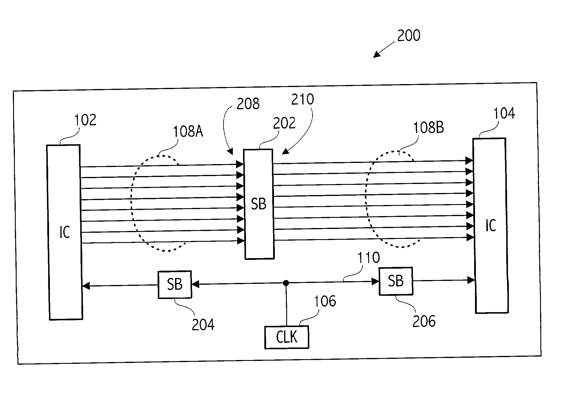
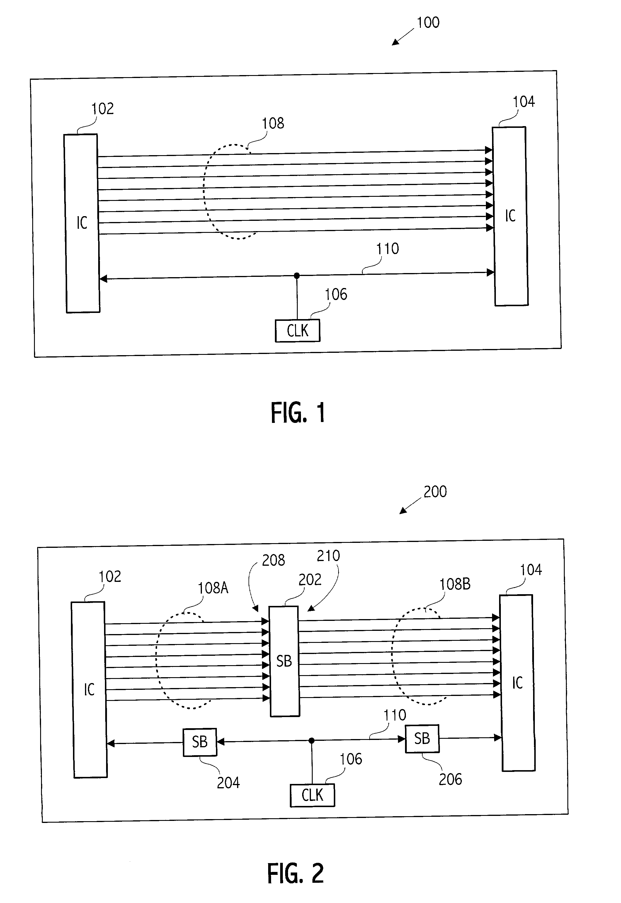
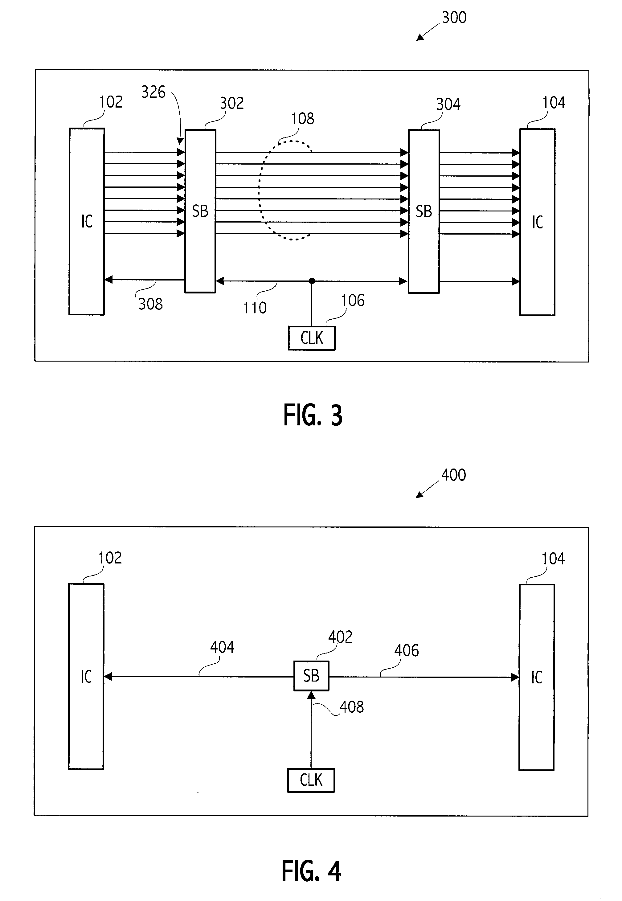
[0032] First in brief overview, the present invention involves the use of a signal buffer IC designed to couple line traces between multiple ICs and to match the impedances of the line traces at the couplings. While not limited thereto, the invention may be more easily understood by its use in support of reducing communication signal reflections (e.g., transmission line effects) and dispersion (e.g., skin effect, dielectric losses, and line trace resistance) between ICs on a PC board.

[0033] For example, referring now to FIG. 1, there is depicted a PC board 100 with a first IC 102 coup...


PUM


Abstract

An improved signal buffer configuration has been developed for transmitting communication signals across line traces between ICs on a printed circuit board, printed wiring board, multi-chip module, integrated circuit carrier or package, or other interconnect substrate. For example, in some realizations, multiple ICs having mismatched input and output impedances are mounted on an printed circuit board and communicate with each other via line traces. A signal buffer IC is placed in-line with the connecting line trace. The buffer is sized to fit within the pitch spacing of the line trace and contains an input impedance control circuit and an output impedance control circuit. These impedance control circuits are adapted to receive a control signal to set the input and output impedances of the buffer to correspond to the impedances of the connecting line traces. In this manner, the impedances between the ICs connected by this line trace are effectively matched and transmission line errors between them are reduced.

Description

[0001] 1. Field of the Invention[0002] The present invention relates to signal transmission systems, and more particularly to techniques for transmitting signals between integrated circuit (IC) devices on printed circuit boards.[0003] 2. Description of the Related Art[0004] Packaged integrated circuits (ICs) are commonly interconnected on printed circuit board (PC boards) by layers of conductors (commonly referred to as line traces). Modem PC boards have as many as 20-24 layers of line traces with pitch spacings as small as 4 MILs. As technology progresses, the signal transfer rate between ICs over these line traces increases as does the length and density of the line traces.[0005] When the impedances between two ICs are mismatched, communication signal integrity between the ICs is degraded by effects such as reflections (e.g., transmission line effect) and dispersion (e.g., skin effect, dielectric losses, and trace resistances). These effects are accentuated with increased signal f...

Claims


Application Information

Patent Timeline
IPC IPC(8): H05K1/02H05K1/18H05K3/22
CPCH05K1/025H05K1/181H05K2201/10689H05K2201/09236H05K2201/10212H05K3/222
Inventor BOSNYAK, ROBERT J.CRUZ-ALBRECHT, JOSE M.
Owner ORACLE INT CORP
Why Eureka
Try Eureka