Method of micromachining a multi-part cavity

Inactive Publication Date: 2002-12-12
APPLIED MATERIALS INC
View PDF27 Cites 67 Cited by
  • Summary
  • Abstract
  • Description
  • Claims
  • Application Information

AI Technical Summary

Problems solved by technology

Because trenches are present at the substrate surface, the thickness of the TEOS SiO.sub.2 collar is not uniform.
While fully effec

Method used


Image

  • Method of micromachining a multi-part cavity
  • Method of micromachining a multi-part cavity
  • Method of micromachining a multi-part cavity

Examples


example two

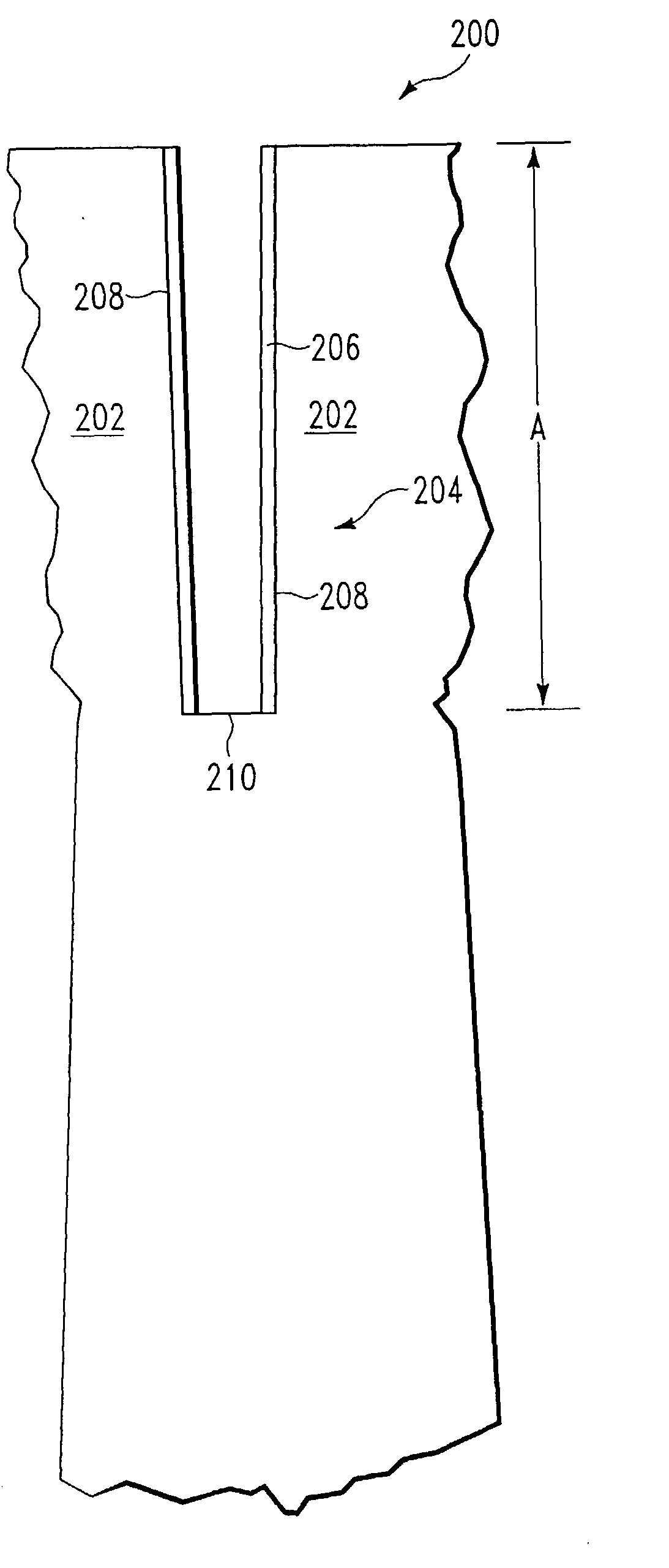
[0163] Referring back to FIG. 8A, a patterned film stack 810 was provided on an upper surface of a single-crystal silicon substrate 802. The patterned film stack included, from top to bottom, a silicon oxide masking layer 808, a silicon nitride etch barrier layer 806, and a gate dielectric layer 804. An upper surface 805 of the single-crystal silicon substrate 802 was exposed.

[0164] In this instance, the gate dielectric layer 804 was a silicon oxide (SiO.sub.x) layer formed by thermal oxidation of the underlying single-crystal silicon substrate 802, using techniques known in the art. The thickness of the gate dielectric layer 804 on the substrate surface 803 was approximately 50 .ANG..

[0165] The silicon nitride layer 806, which functions as an etch barrier layer throughout the method of the invention, was formed to have an initial thickness of approximately 2200 .ANG.. Other possible materials that can serve as etch barrier layers include, without limitation, silicon dioxide, titani...


PUM

PropertyMeasurementUnit
Fractionaaaaaaaaaa
Fractionaaaaaaaaaa
Percent by volumeaaaaaaaaaa

Abstract

The present disclosure pertains to our discovery of a particularly efficient method for etching a multi-part cavity in a substrate. The method provides for first etching a shaped opening, depositing a protective layer over at least a portion of the inner surface of the shaped opening, and then etching a shaped cavity directly beneath and in continuous communication with the shaped opening. The protective layer protects the etch profile of the shaped opening during etching of the shaped cavity, so that the shaped opening and the shaped cavity can be etched to have different shapes, if desired. In particular embodiments of the method of the invention, lateral etch barrier layers and/or implanted etch stops are also used to direct the etching process. The method of the invention can be applied to any application where it is necessary or desirable to provide a shaped opening and an underlying shaped cavity having varying shapes. The method is also useful whenever it is necessary to maintain tight control over the dimensions of the shaped opening.

Description

[0001] 1. Field of the Invention[0002] The present invention pertains to a method of micromachining a multi-part cavity in a substrate, wherein different parts of the cavity may be formed to have different shapes. The present invention also pertains to a method of forming a multi-part cavity in a semiconductor substrate, for the purpose of manufacturing a semiconductor device.[0003] 2. Brief Description of the Background Art[0004] Numerous methods for preparing semiconductor devices which include a trench in a silicon crystal silicon or polycrystalline silicon substrate have been described in the art. A few of these methods are described below.[0005] U.S. Pat. Nos. 4,895,810 and 5,182,234, issued Jan. 23, 1990 and Jan. 26, 1993, respectively, to Meyer and Hollinger et al., disclose methods for creating a device structure where a trench is formed in an upper silicon surface and a source conductive layer is deposited to electrically contact a source region while a gate conductive laye...

Claims


Application Information

Patent Timeline
IPC IPC(8): B81C1/00H01L21/3065H01L21/308H01L21/8242
CPCH01L21/3065H01L21/3086H01L27/1087B81B2203/033B81C1/00119B81B2201/052B81B2203/0315B81C2201/016H10B12/0387
Inventor PODLESNIK, DRAGANLILL, THORSTENCHINN, JEFFPAN, SHAOHER X.KHAN, ANISULLI, MAOCHENGWANG, YIQIONG
Owner APPLIED MATERIALS INC
Why Eureka
Try Eureka