Optical detector device

a detector device and optical technology, applied in the field of optical detector devices, can solve the problems of not providing images with high image quality, high aperture ratio,

Inactive Publication Date: 2002-12-19
HAMAMATSU PHOTONICS KK
View PDF3 Cites 21 Cited by
  • Summary
  • Abstract
  • Description
  • Claims
  • Application Information

AI Technical Summary

Benefits of technology

[0022] Furthermore, the first and second optical detector devices according to the present invention are further equipped with a CDS (Correlated Double Sampling) circuit, which outputs a CDS output value according to the amount of change in the integrator output value. This eliminates the influence of any offset variation that is included in the integrator output that is outputted from the integrator circuit. In addition to this, preferably an optical change range detector circuit, which detects whether or not the CDS output value is within a specific range, is also provided.
[0025] In each of these cases, the optical detector device can detect increases and decreases in the light intensity for each individual pixel in the image, and is thus able to extract moving objects. The scope of the circuit required for each pixel in this optical detector device is substantially smaller than in conventional technologies. In particular, when the junction capacitance of the optical detector element is used as the capacitor, the size of the circuit is even smaller. Consequently, in this optical detector device, the surface area on the chip required for the circuit part for each pixel is small, so the aperture ratio for each pixel is large, producing superior optical response characteristics.

Problems solved by technology

Consequently, the area required on the chip for the circuitry for each pixel in this optical detector device has been large, and, as a result, this optical detector device has had the fatal flaw that it could not achieve a high aperture ratio, which determines the light response characteristics of the sensor, and thus could not provide images with high image quality.

Method used


Image

  • Optical detector device
  • Optical detector device
  • Optical detector device

Examples


first embodiment

[0037] an optical detector device according to the present invention will be explained below.

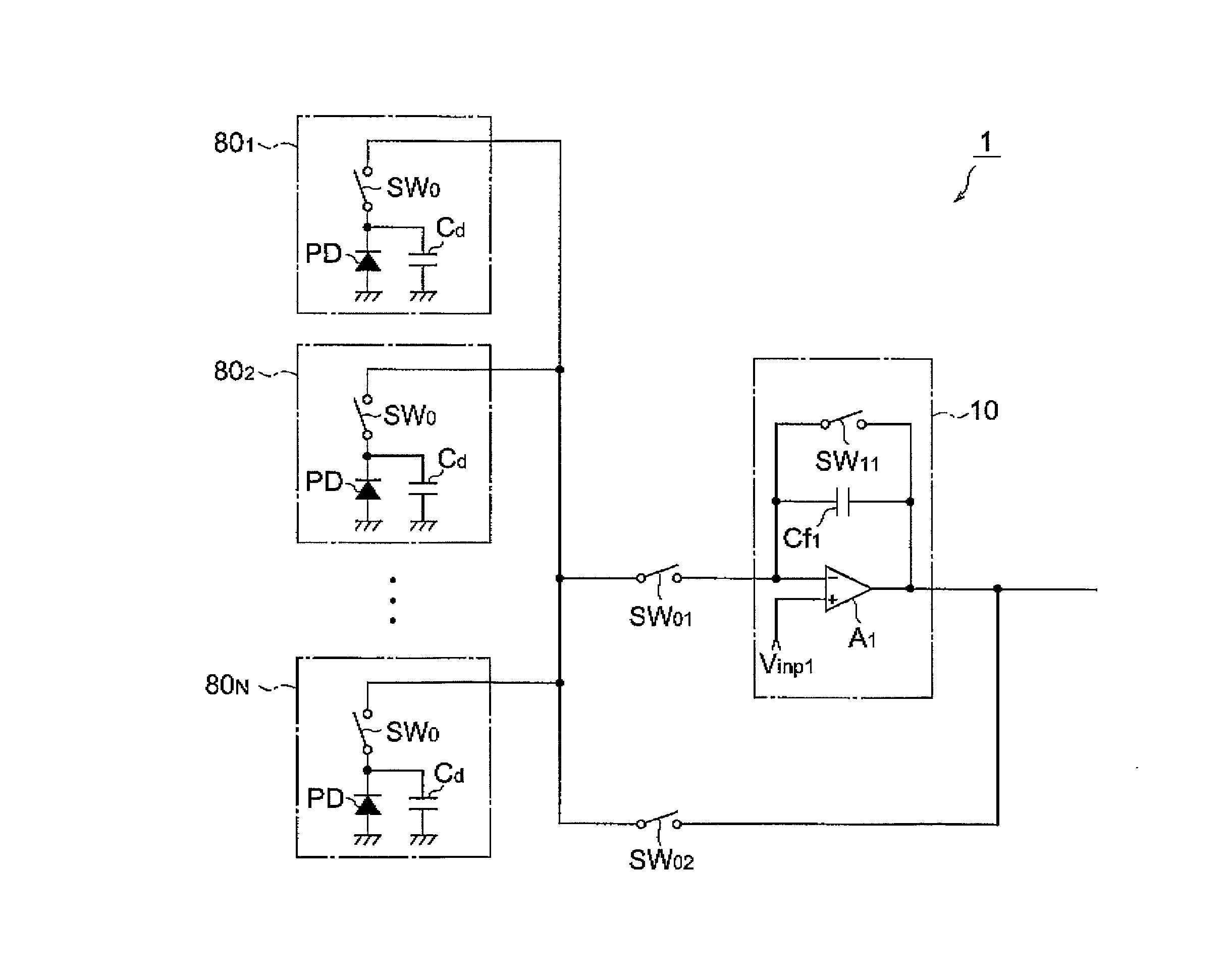
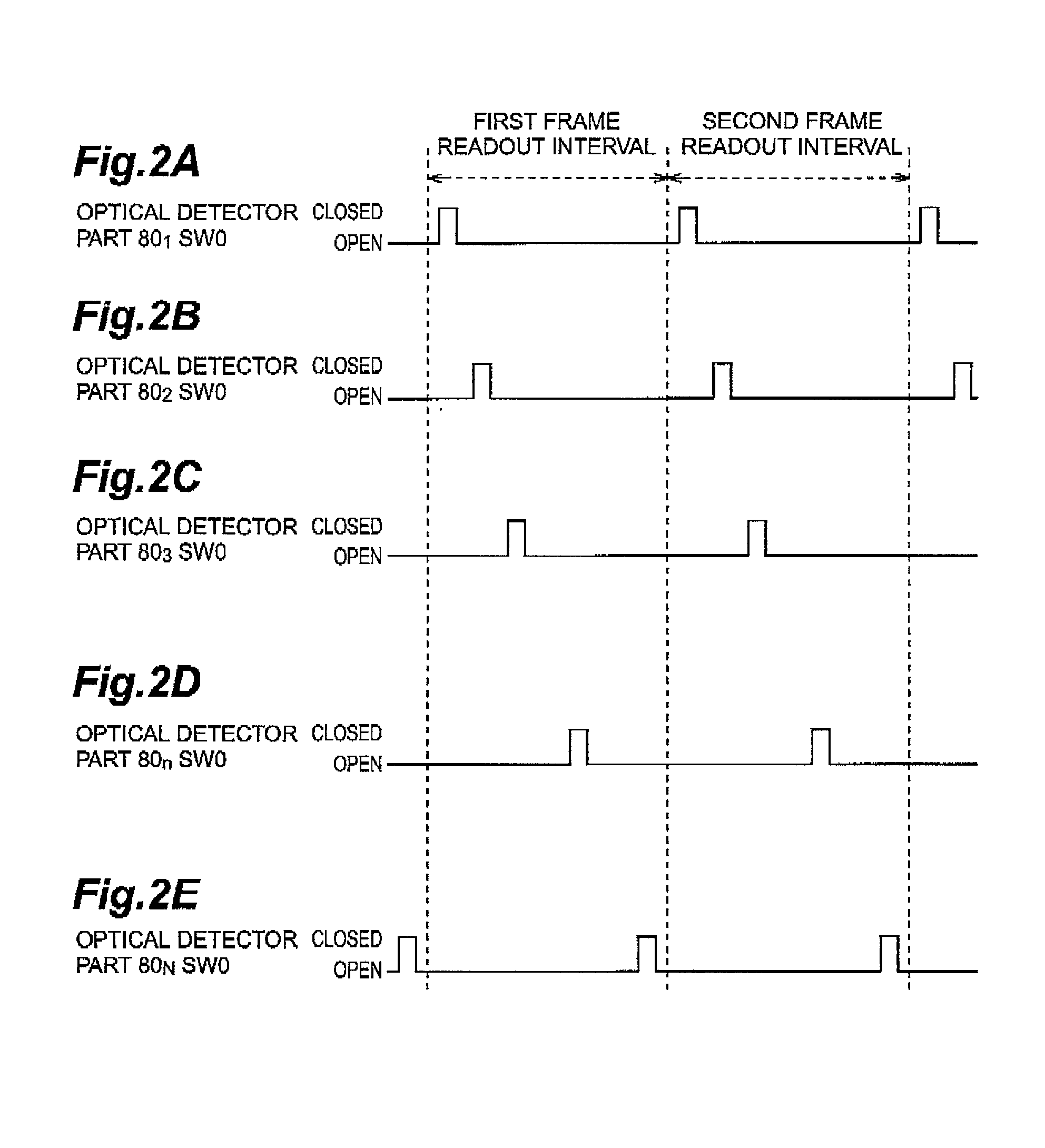
[0038] FIG. 1 is a circuit diagram of an optical detector device 1 according to the first embodiment. This optical detector device 1 comprises N optical detector parts 80.sub.1 through 80.sub.N, an integrator circuit 10, a first switch SW.sub.01, and a second switch SW.sub.O2.

[0039] The N optical detector parts 80.sub.1 to 80.sub.N each have a photodiode PD, a capacitor C.sub.d and a switch SW.sub.0. The anode terminals of the photodiodes PD are connected to ground. The cathode terminals of the photodiodes PD are connected through the capacitor C.sub.d and through the switch SW.sub.0 to the switch SW.sub.01 and the switch SW.sub.02.

[0040] The capacitors C.sub.d of each of the N optical detector parts 80.sub.1 to 80.sub.N all have the same capacitance. Furthermore, the capacitors C.sub.d are the junction capacitances of the photodiodes PD, or may be equipped separately.

[0041] An operational a...

second embodiment

[0070] Next a second embodiment of the optical detector device according to the present invention will be explained.

[0071] FIG. 4 is a circuit diagram of an optical detector device 2 according to the second embodiment.

[0072] The optical detector device 2 according to the second embodiment, when compared to the optical detector device of the first enbodiment, has a different circuit structure in the integrator circuit 10.

[0073] In the integrator circuit 10 of the optical detector device 2 an amplifier A.sub.1, an integrator circuit capacitor C.sub.f1, and a switch SW.sub.11 are connected in parallel with each other between the input terminal and the output terminal, connected in parallel to a switch SW.sub.12 (a capacitance switching means) and an integrator circuit capacitor C.sub.f2, which are connected in series with each other. The amplifier A.sub.1 is connected so that its inverted input terminal (-) is connected to the switch SW.sub.01, and its non-inverted input terminal (+) i...

third embodiment

[0082] A third embodiment of an optical detector device according to the present invention will be explained next.

[0083] FIG. 6 is a circuit diagram of an optical detector device 3 according to the third embodiment.

[0084] The optical detector device 3 according to the third embodiment, when compared with the second embodiment, has an added CDS circuit 20 and a sample and hold circuit 30.

[0085] The CDS circuit 20 has a capacitor (capacitive element) C.sub.21 and an operational amplifier A.sub.2 in series between the input terminal and the output terminal. Additionally, a switch SW.sub.2 and a capacitor (capacitive element) C.sub.22 are connected in parallel between the input terminals of the amplifier A.sub.2. The CDS circuit 20 is initialized (reset) by discharging the accumulated charge of the capacitor C.sub.22 when the switch SW.sub.2 is closed.

[0086] On the other hand, in the CDS circuit 20, when the switch SW.sub.2 is open, the charge that is inputted through the capacitor C.su...


PUM


Abstract

Each of N optical detector parts 801 to 80N has a photodiode PD, a capacitor Cd and a switch SW0. An amplifier A1, an integrator circuit capacitor Cf1, and a switch SW11 , are connected in parallel between the input terminal and the output terminal of an integrator circuit 10. The capacitance of the integrator circuit capacitance C11 is equal to the capacitance of the capacitor Cd in each of the N optical detector parts 801 to 80N. A switch SW01, is equipped between the input terminal of the integrator circuit 10 and the switch SW0 for each of the N optical detector parts 801 to 80N. A switch SW02 is equipped between the output terminal of the integrator circuit 10 and the switch SW0 in each of the N optical detector parts 801, to 80N.

Description

[0001] This is a continuation-in-part application of application Ser. No. PCT / JP00 / 08175 filed on Nov. 20, 2000, now pending.[0002] 1. Field of the Invention[0003] The present invention relates to an optical detector device that extracts moving objects in incident optical images.[0004] 2. Related Background Art[0005] Optical detector devices fabricated by CMOS technologies can be built for a low cost on a single chip that includes the A / D converter circuits and the peripheral digital circuitry. Because of this, optical detector devices have been developed that, rather than just detecting light, include a variety of processing functions (for example, outline extraction or moving object extraction) on a single chip.[0006] An optical detector device that has a moving object extraction function is described, for example, in Ishiwata, et al., "CMOS lmage Sensor for the Recognition of Three-Dimensional Gestures," Image Information Media Association Technical Reports, Vol. 23, No. 30, pgs ...

Claims


Application Information

Patent Timeline
Patent Type & Authority Applications(United States)
IPC IPC(8): G01J1/46G06T7/20H04N5/335H04N5/351H04N5/357H04N5/363H04N5/369H04N5/374
CPCG01J1/46H04N5/335H04N3/155H04N25/77H04N25/00
Inventor MIZUNO, SEIICHIROMUKOZAKA, NAOHISATOYODA, HARUYOSHI
Owner HAMAMATSU PHOTONICS KK
Why Eureka
Try Eureka