Avalanche photodiode array biasing device and avalanche photodiode structure

Inactive Publication Date: 2002-12-26
APTINA IMAGING CORP
View PDF6 Cites 39 Cited by
  • Summary
  • Abstract
  • Description
  • Claims
  • Application Information

AI Technical Summary

Problems solved by technology

A limiting factor in the use of avalanche photodiode devices is the careful control that must be exercised over the electric field generated by the applied reverse bias.
Unfortunately, the device gain value cannot be easily measured.
If the gain is too low, the noise of the preamplifi

Method used


Image

  • Avalanche photodiode array biasing device and avalanche photodiode structure
  • Avalanche photodiode array biasing device and avalanche photodiode structure
  • Avalanche photodiode array biasing device and avalanche photodiode structure

Examples


Embodiment Construction

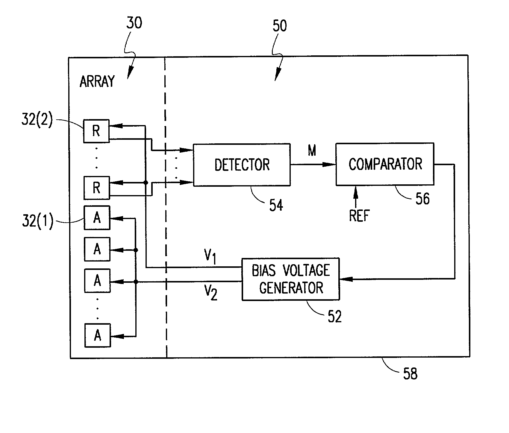
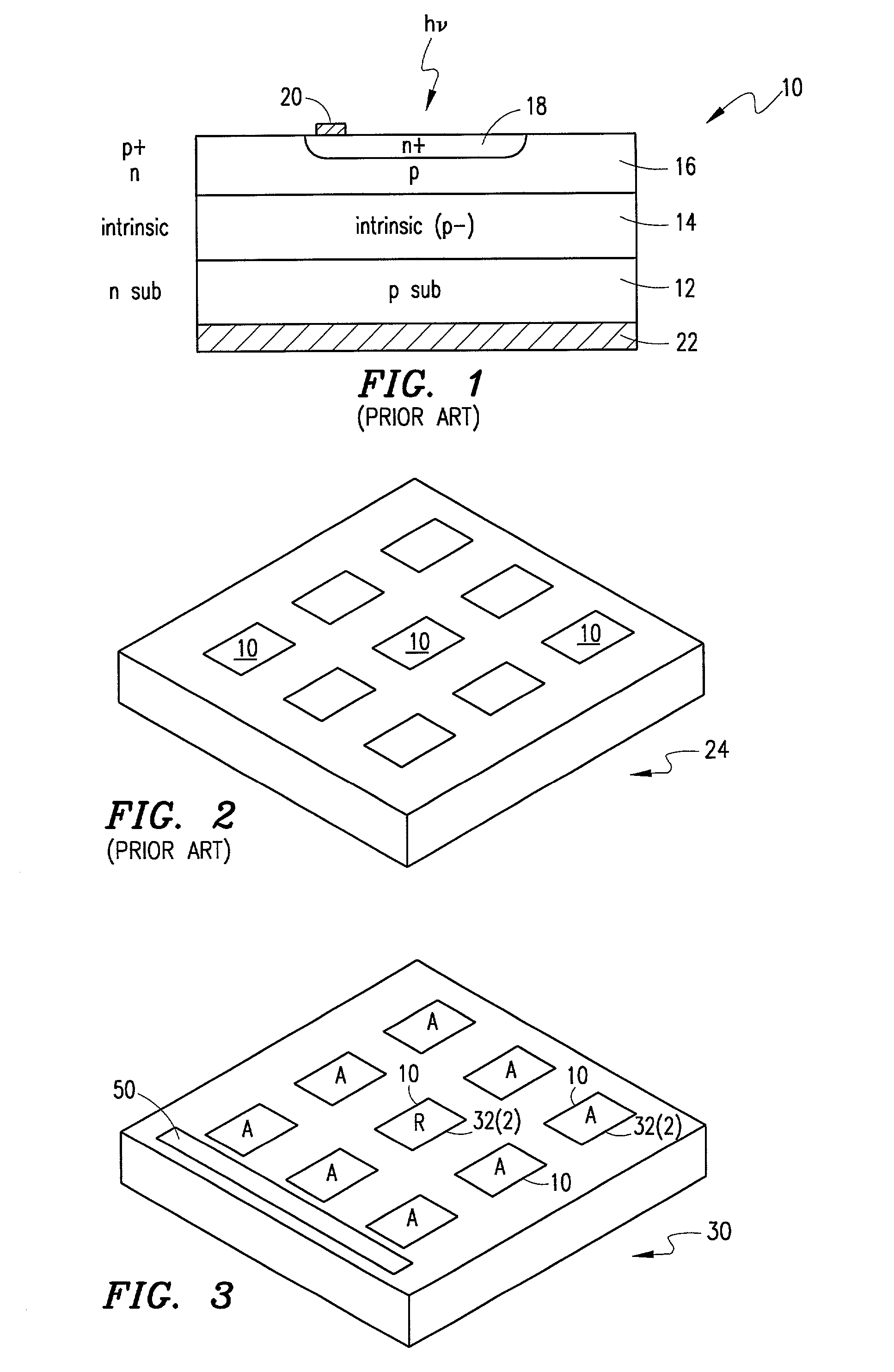
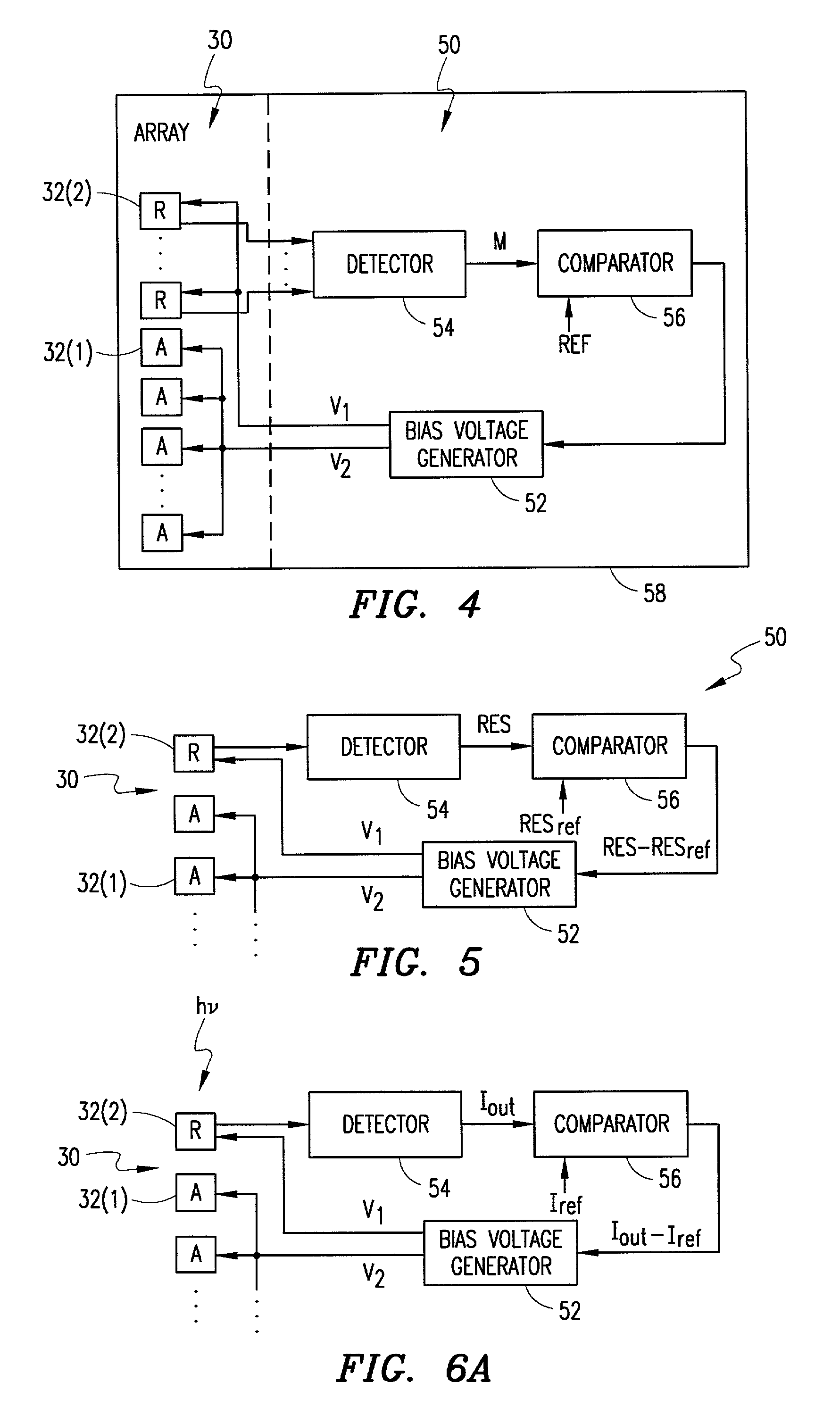
[0024] FIG. 3 is a perspective view of an avalanche photodiode array 30 in accordance with an embodiment of the invention. The array 30 includes a plurality of diode devices 32 that may be of any known type including the type illustrated in FIG. 1 (and / or also the type shown in FIGS. 9A-9C to be discussed). These included devices 32 may be classified into two groups: a first group of devices 32(1) (designated with an "A") which comprise active photodiodes for the array 30; and a second group of devices 32(2) (designated "R") which comprise reference diodes for the array. In this context, the phrase "active photodiodes" as disclosed and claimed refers to those included photodiode devices 32(1) that are used to actively measure and / or detect light and to output signals indicative of that light for processing in connection with the operation of the array 30 in a certain user application. The phrase "reference diodes," on the other hand, as disclosed and claimed refers to those included...


PUM


Abstract

A photodiode array includes a plurality of arrayed individual diode devices. The arrayed diode devices include at least one active photodiode and at least one reference diode. A bias control circuit for the array monitors operation of the reference diode at an applied first bias voltage and adjusts that applied first bias voltage until optimal reference diode operation is reached. A second bias voltage having predetermined relationship to the first bias voltage is applied to the active photodiode to optimally configure array operation. More specifically, an operational characteristic of the reference diode at the first bias voltage is monitored and compared to a reference value. As a result of this comparison, the circuit adjusts the applied first and second bias voltage in order to drive the reference diode measured characteristic to substantially match the reference value. The operational characteristic that is measured may comprise reference diode responsivity or reference diode output current, and may be based on either electrical or optical device operation. Each avalanche photodiode semiconductor structure may have a conventional reverse biased pn junction semiconductor structure providing a high field region as is well known in the art. An enhanced semiconductor structure may also be utilized wherein a heavily doped layer that is physically separate from the pn junction is also included to provide a source of charge carriers that are swept into the high field region.

Description

[0001] 1. Technical Field of the Invention[0002] The present invention relates to avalanche photodiodes and, in particular, to arrays of avalanche photodiodes.[0003] 2. Description of Related Art[0004] An avalanche photodiode (APD) is a semiconductor photosensor device capable of light detection. It is especially useful in low, weak or reduced light applications as the avalanche phenomenon utilized by the device provides for a significant degree of amplification. Avalanche occurs when carriers generated by photon induced free carrier generation in a light receiving area of the device are introduced into a high electric field area formed in a highly reverse biased (near breakdown voltage) semiconductor pn junction. The introduced carriers collide with neutral atoms to release other carriers by impact ionization. This collision process is then repeated and repeated in an avalanche fashion to effectively amplify the limited number of carriers that were initially produced by photon indu...

Claims


Application Information

Patent Timeline
IPC IPC(8): H01L27/146H01L31/02H01L31/107
CPCH01L27/14643H01L31/107H01L31/02027
Inventor NISHIMURA, KEN A.LEMOFF, BRIAN E.HOLLENHORST, JAMES N.
Owner APTINA IMAGING CORP
Why Eureka
Try Eureka