Light emitting device and method of manufacturing the same

a technology of light emitting device and manufacturing method, which is applied in the direction of identification means, instruments, discharge tubes, etc., can solve the problems of clogging nozzles, shooting misses the target, and off-course fligh

Inactive Publication Date: 2003-01-09
SEMICON ENERGY LAB CO LTD
View PDF3 Cites 37 Cited by
  • Summary
  • Abstract
  • Description
  • Claims
  • Application Information

AI Technical Summary

Problems solved by technology

In addition, the ink jet method has the problem of `off-course flight`; the ink jet method sends a jet of polymeric material into the air and, if the distance between the application target surface and the nozzle of the ink jet head is not set appropriately, the shot misses the target.
Furthermore, the ink jet method ejects ink containing an organic compound from a nozzle and a problem of a clogged nozzle when the ink has high viscosity occurs.
However, it is impossible to perform high-precision patterning with a nozzle having large diameter.
Therefore, the ink jet method is not the optimum film formation method, nor an easy method.

Method used


Image

  • Light emitting device and method of manufacturing the same
  • Light emitting device and method of manufacturing the same
  • Light emitting device and method of manufacturing the same

Examples


embodiment 1

[0092] [Embodiment 1]

[0093] In this embodiment, an active matrix light emitting device is manufactured in accordance with a manufacturing method of the present invention.

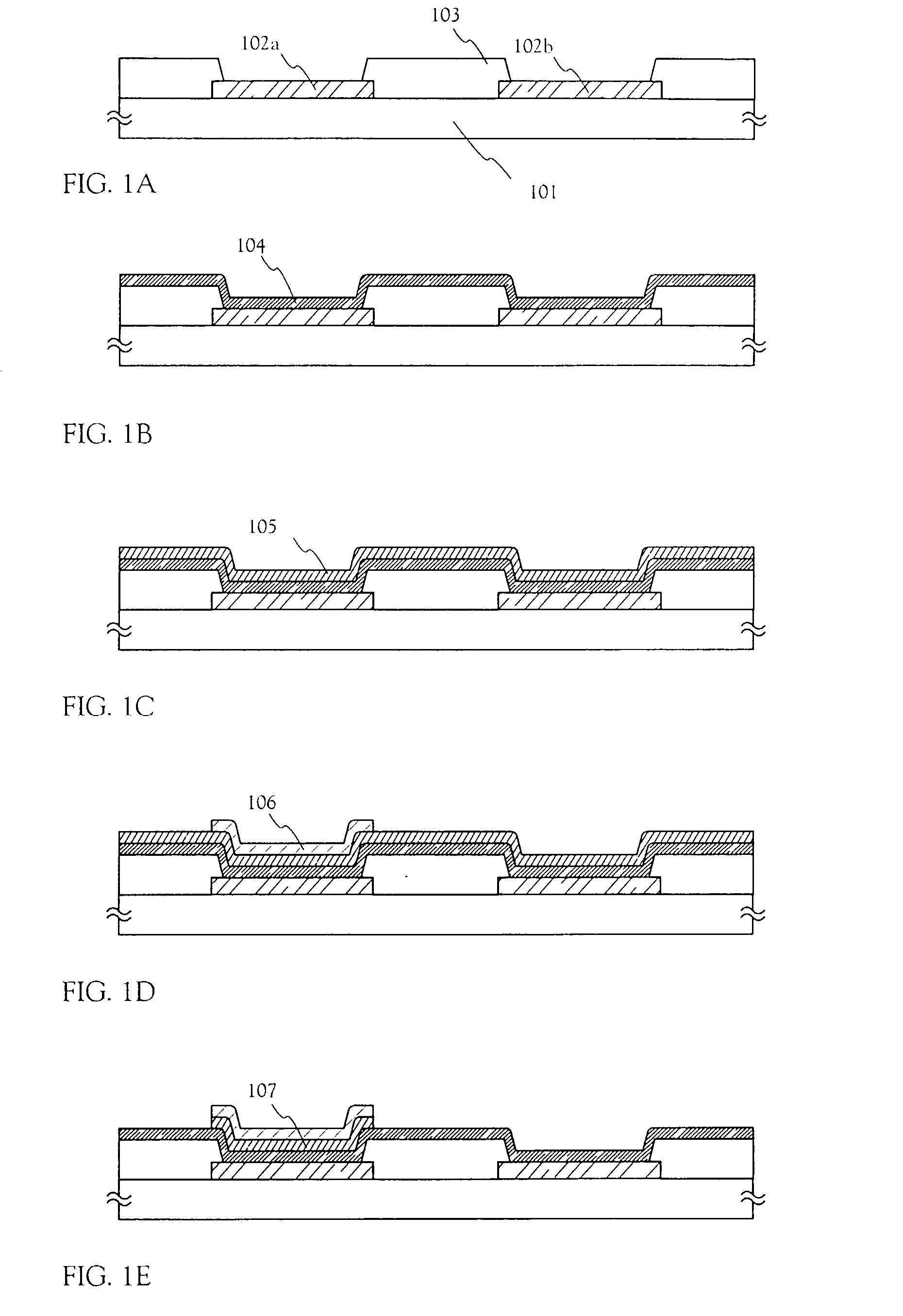
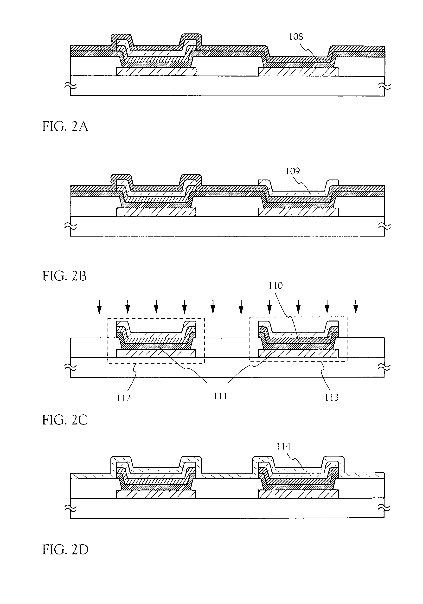
[0094] FIG. 4A shows a part of a pixel portion 401 formed on a substrate. The pixel portion 401 has a plurality of pixels 402 that form a matrix. FIG. 4B is a sectional view taken along the dotted line P-P' in the pixel portion 401 of FIG. 4A.

[0095] In FIG. 4B, a TFT 404 for driving a light emitting element (hereinafter referred to as current controlling TFT) is formed on a substrate 403.

[0096] This embodiment uses a glass substrate as the substrate 403 but any material can be employed for the substrate 403 as long as it can transmit light. The current controlling TFT 404 can be manufactured by a known TFT manufacturing method. The current controlling TFT 404 may be a top gate TFT or a bottom gate TFT.

[0097] An interlayer insulating film 405 is formed from an insulating material on the current controlling TFT 404. T...

embodiment 2

[0116] [Embodiment 2]

[0117] Embodiment 1 shows an example of choosing a luminous polymeric organic compound that is soluble in an aprotic solvent from polymeric organic compounds that can be used to form organic compound layers. However, the present invention can employ a polymeric organic compound that has little or no Solubility to an aprotic solvent if it can be dispersed in the aprotic solvent. It is also possible to mix an organic compound that does not emit light but has other functions in an organic compound layer. Organic compounds that can be used in the present invention are listed below.

[0118] Functions that the organic compounds in the present invention have other than light emission can be hole transportation function and electron transportation function. These materials are not necessarily polymeric organic compounds but may be low molecular weight organic compounds.

[0119] Examples of those compounds which are known as the material having the hole transportation, and w...

embodiment 3

[0126] [Embodiment 3]

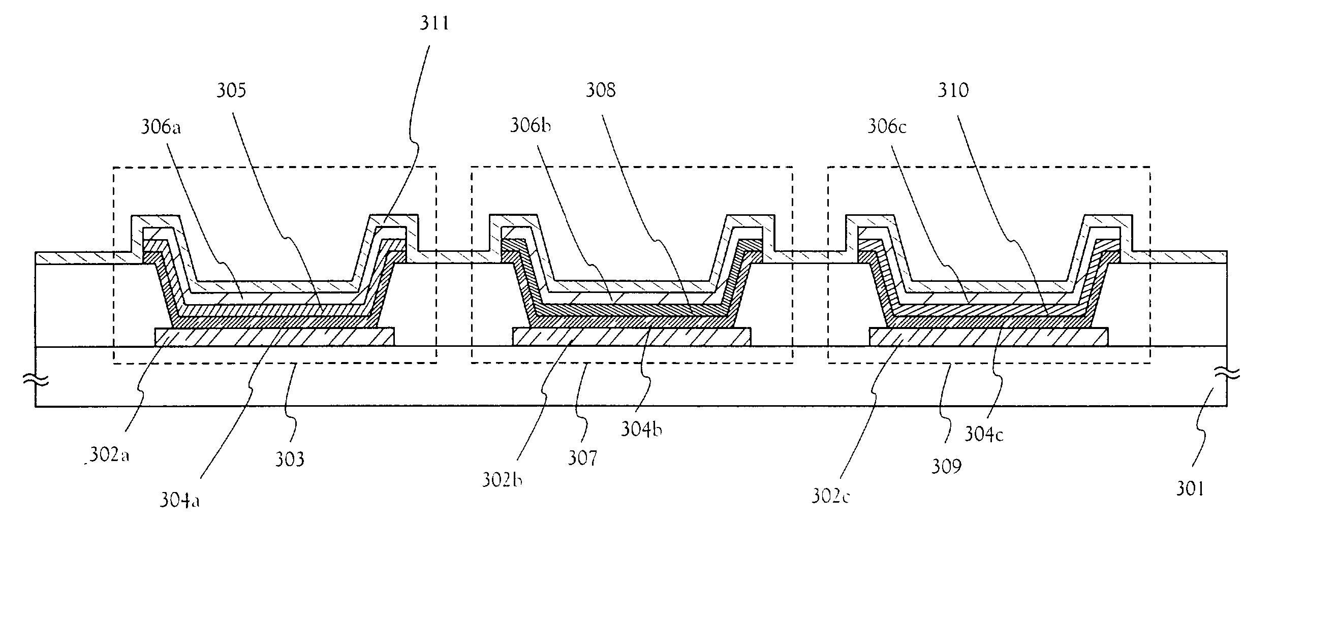
[0127] FIG. 8A shows a detailed top structure of the pixel portion of the light emitting device manufactured in accordance with the present invention in Embodiment 1. FIG. 8B shows a circuit diagram thereof. The same reference symbols are used in FIGS. 8A and 8B so that cross reference can be made.

[0128] In this embodiment, a TFT in a region denoted by 800 is called a switching TFT and a TFT in a region denoted by 805 is called a current controlling TFT. The switching TFT 800 has a source connected to a source signal line 803 and has a drain connected to a drain wiring line 804. The drain wiring line 804 is electrically connected to a gate electrode 806 of the current controlling TFT 805.

[0129] The switching TFT 800 has a channel formation region, which is in contact with the source and drain regions of the switching TFT 800. The channel formation region overlaps a gate electrode 801 (801a and 801b) that is electrically connected to a gate signal line 802.

[0130]...


PUM

PropertyMeasurementUnit
thicknessaaaaaaaaaa
thicknessaaaaaaaaaa
thicknessaaaaaaaaaa

Abstract

An easier method is provided to manufacture a light emitting device that can display a full-color image using a polymeric organic compound. In the present invention, some of polymeric organic compounds are dissolved in a protic solvent while the others are dissolved in an aprotic solvent and the obtained solutions are applied to form organic compound films having laminate structures. A conductive film to serve as an etching stopper is formed on the organic compound films, so that portions of the organic compound films that do not overlap the conductive film are etched away. By using wet etching and dry etching in combination, different organic compound films each composed of a plurality of polymeric organic compounds can be formed in different light emitting elements on the same substrate.

Description

[0001] 1. Field of the Invention[0002] The present invention relates to a light emitting device with a light emitting element that emits fluorescent light or phosphorescent light upon application of electric field to a pair of electrodes of the element which sandwich a film containing an organic compound (the film is hereinafter referred to as organic compound layer), and to a method of manufacturing the light emitting device. In the present invention, the term tight emitting device includes to an image display device that uses a light emitting element Also, the following modules are all include in the definition of the light emitting device: a module obtained by attaching to a light emitting element a connector such as an FPC (flexible printed circuit), a TAB (tape automated bonding) tape, or a TCP (tape carrier package); a module in which a printed wiring board is provided at an end of the TAB tape or the TCP; and a module in which an IC (integrated circuit) is directly mounted to...

Claims


Application Information

Patent Timeline
Patent Type & Authority Applications(United States)
IPC IPC(8): G09F9/00H05B33/10G09F9/30H01L27/32H01L51/00H01L51/30H01L51/50H05B33/12H05B33/22
CPCH01L27/3211H01L51/0036H01L51/0037H01L51/0038H01L51/0039H01L51/0059H01L51/0077H01L51/0081H01L51/0084H10K59/35H10K85/114H10K85/115H10K85/113H10K85/1135H10K85/631H10K85/30H10K85/341H10K85/324H10K50/822H10K50/824H10K71/00
Inventor OGINO, KIYOFUMISHIBATA, NORIKO
Owner SEMICON ENERGY LAB CO LTD
Why Eureka
Try Eureka