Semiconductor light-emitting device and methods for fabricating the same

Inactive Publication Date: 2003-05-01
EPISTAR CORP
View PDF0 Cites 23 Cited by
  • Summary
  • Abstract
  • Description
  • Claims
  • Application Information

AI Technical Summary

Problems solved by technology

Thus the fabricating process of the device is complicated, resulting in time-consuming and costly manufacturing process.
As to the light-emitting diode having three emission layers in JP 232627/1997 A, the fabricating process of three emission layers is complicated, resulting in time-consuming and costly manufacturing process.
In addition, the emission layer composed of InGaN needs to contain a large proportion of In composition in order to emit red light, but such an emission layer

Method used


Image

  • Semiconductor light-emitting device and methods for fabricating the same
  • Semiconductor light-emitting device and methods for fabricating the same
  • Semiconductor light-emitting device and methods for fabricating the same

Examples


first embodiment

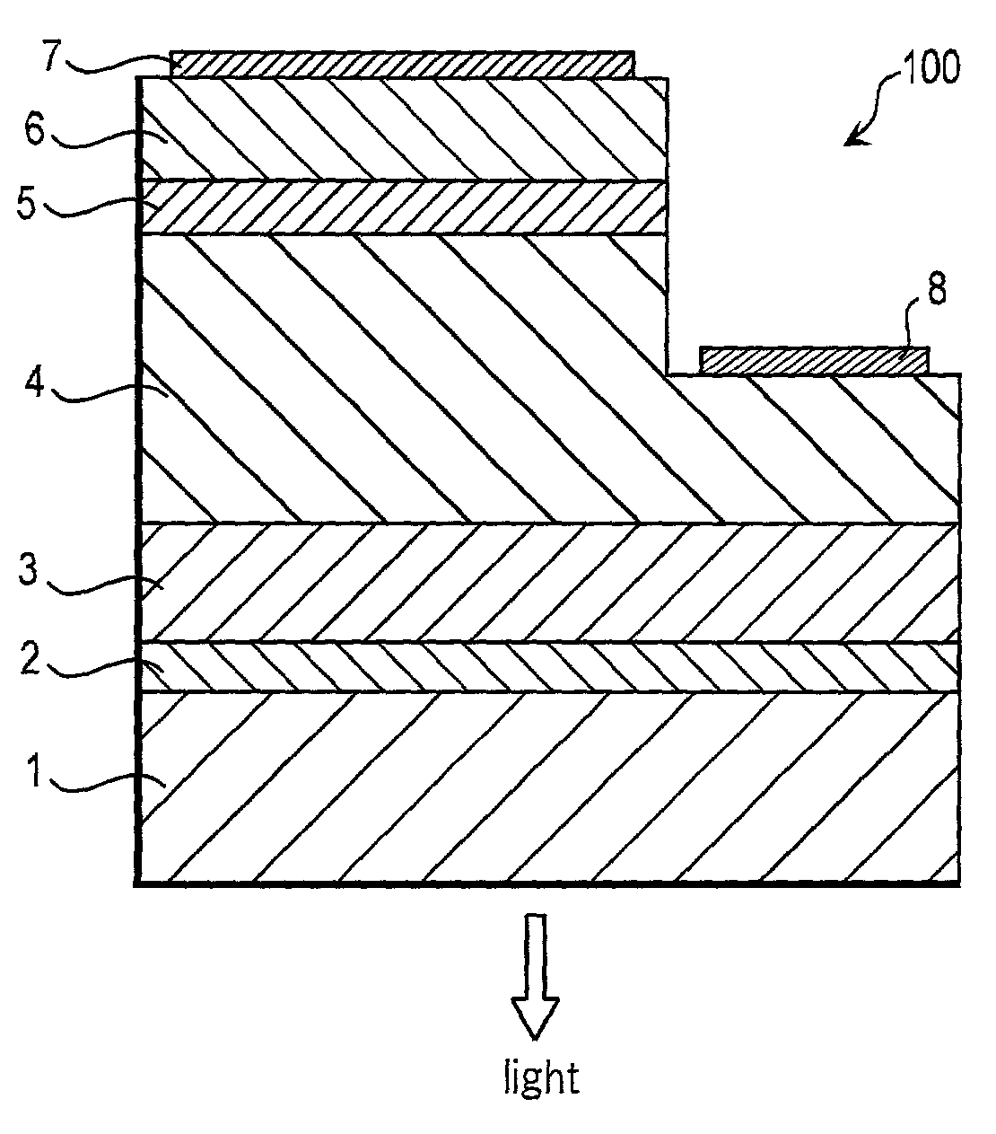
[0042] FIG. 1 is a cross sectional view schematically illustrating a light-emitting diode in a first embodiment according to the present invention.

[0043] A light-emitting diode 100 shown in FIG. 1 is fabricated by growing layers 2-6 (as will be described later) on a sapphire substrate 1 by MOCVD (Metal Organic Chemical Vapor Deposition) method.

[0044] Specifically, a buffer layer 2 composed of Al.sub.0.5Ga.sub.0.5N is grown to about 15 nm in thickness on C (0001) surface of the sapphire substrate 1. An Si(Silicon)-doped GaN fluorescent layer 3 of 1 .mu.m in thickness is formed on the buffer layer 2.

[0045] The Si-doped GaN fluorescent layer 3 is doped excessive amount of Si by increasing a flow of silane gas (SiH.sub.4), compared with the conventional Si-doped GaN fluorescent layer. Such a Si-doped GaN fluorescent layer 3 exhibits good fluorescent properties.

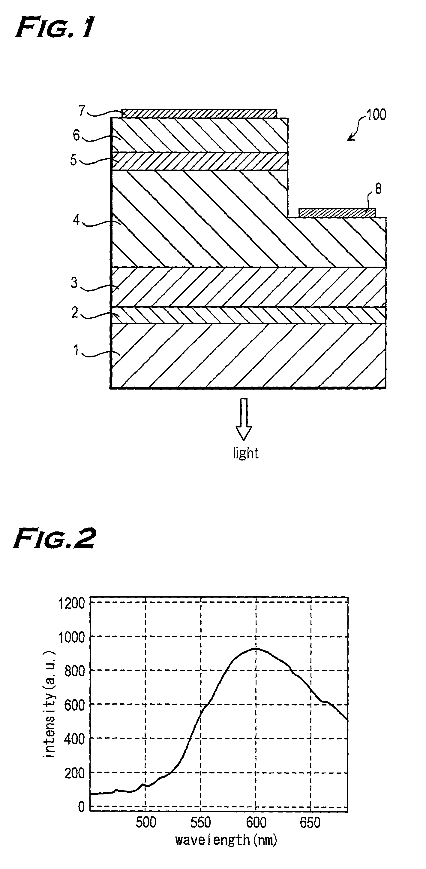
[0046] When the above described Si-doped GaN fluorescent layer 3 is irradiated by He--Cd laser of 325 nm in wavelength and excit...

second embodiment

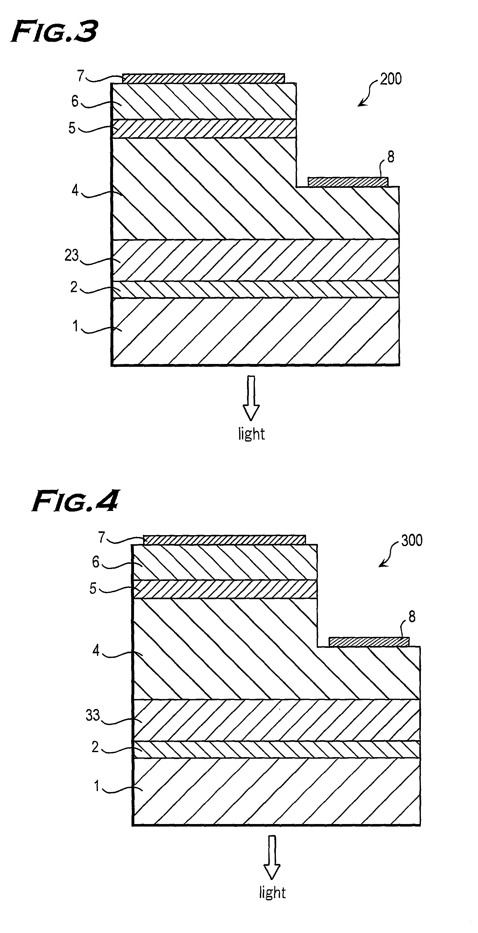
[0079] FIG. 3 is a cross sectional view illustrating a light-emitting diode of a second embodiment in the present invention.

[0080] A light-emitting diode 200 shown in FIG. 3 has the same structure as the light-emitting diode 100 shown in FIG. 1 except that an undoped GaN fluorescent layer 23 of approximately 1 .mu.m in thickness is formed, instead of the Si-doped GaN fluorescent layer 3. Such a light-emitting diode 200 is fabricated in the same method as the light-emitting diode 100 with the exceptions as follows.

[0081] In the fabrication of the light-emitting diode 200, an undoped GaN fluorescent layer 23 is grown to 1 .mu.m in thickness as keeping a substrate at 1150.degree. C. after forming a buffer layer 2.

[0082] When NH.sub.3 and TMGa are supplied to grow the undoped GaN fluorescent layer 23, the mmole ratio of a flow of NH.sub.3 to a flow of TMGa (V / III) is set smaller than that for the conventional undoped GaN layer with sufficient good crystallinity.

[0083] While the mole rat...

third embodiment

[0091] FIG. 4 is a cross sectional view illustrating a light-emitting diode of a third embodiment in the present invention.

[0092] A light-emitting diode 300 shown in FIG. 4 has the same structure as the light-emitting diode 100 shown in FIG. 1 except that a C (carbon)-doped GaN fluorescent layer 33 of approximately 1 .mu.m in thickness is formed, instead of the Si-doped GaN fluorescent layer 3. Such a light-emitting diode 300 is fabricated in the same method as the light-emitting diode 100 with the exceptions as follows.

[0093] In the fabrication of the light-emitting diode 300, a C-doped GaN fluorescent layer 33 is grown to 1a m in thickness as keeping a substrate at temperature of 1150.degree. C. after forming a buffer layer 2.

[0094] In order to grow the C-doped GaN fluorescent layer 33, CH.sub.4 of 10 sccm, which is carbon source, is supplied as well as NH.sub.3 and TMGa. The mole ratio of a flow of NH.sub.3 to a flow of TMGa (V / III) is set 5000. The C-doped fluorescent layer fabr...


PUM


Abstract

This invention provides a light-emitting diode which is capable of extracting white light, manufactured readily and highly reliable. The light-emitting diode is fabricated by laminating a buffer layer 2, an Si (silicon)-doped GaN fluorescent layer 3, an n-GaN layer 4, an MQW emission layer 5 and a p-GaN layer 6 on a sapphire substrate 1 in this order. The Si-doped GaN fluorescent layer 3 is doped higher concentration of Si (silicon) than a conventional Si-doped GaN layer with sufficient good crystallinity. Such a Si-doped GaN fluorescent layer is excited by blue light generated in the MQW emission layer and emits yellow light. The yellow light is the complement for the blue light generated in the MQW emission layer. White light can be obtained by blending and extracting both of blue light and yellow light.

Description

[0001] 1. Field of the Invention[0002] The invention relates to a semiconductor light-emitting device comprising of a group III-V nitride base semiconductor (hereafter referred to as a nitride base semiconductor) such as BN(boron nitride), GaN(gallium nitride), AlN(aluminum nitride), InN(indium nitride), TlN(thallium nitride), or crystal mixtures of these nitrides, and capable of emitting white light, and a method of fabricating the semiconductor light-emitting device.[0003] 2. Description of Prior Art[0004] White light-emitting devices using light-emitting diodes are under development in order to invent a white light source having a low power consumption, high reliability and a long-life.[0005] For example, a light-emitting device in which three light-emitting diodes emitting light beams of primary colors, red, green and blue respectively are arranged on one stem has been known. Such a light-emitting device is capable of emitting white light by blending red light, green light and b...

Claims


Application Information

Patent Timeline
IPC IPC(8): H01L33/08H01L33/12H01L33/32H01L33/50
CPCH01L33/32H01L33/08
Inventor TOMINAGA, KOUJI
Owner EPISTAR CORP
Why Eureka
Try Eureka