Method of manufacturing semiconductor device for evaluation capable of evaluating crystal defect using in-line test by avoiding using preferential etching process

a semiconductor device and crystal defect technology, applied in the direction of luminescent dosimeters, optical radiation measurement, instruments, etc., can solve the problems of junction characteristics, junction leakage increase, and various device characteristics are degraded

Inactive Publication Date: 2003-06-19
RENESAS TECH CORP
View PDF0 Cites 8 Cited by
  • Summary
  • Abstract
  • Description
  • Claims
  • Application Information

AI Technical Summary

Problems solved by technology

Crystal defects which are likely to occur during manufacture of a semiconductor substrate, or are induced in a semiconductor substrate due to a manufacturing process for a semiconductor device, cause degradation of various device characteristics such as junction characteristics (i.e., increase in junction leakage), on one hand.
On the other hand, however, crystal defects, provided that the density or location thereof is controlled, are utilized as gettering sites for removing metals contained in a region where a device is to be formed.
In evaluating crystal defects generated within the substrates having the aforementioned structures, use of the conventional evaluation method which entails a preferential etching process has caused some problems.
Further, microroughness is liable to be caused in a surface of the thin film SOI layer, an interface between the thin film SOI layer and the buried oxide layer, a surface of the thin film surface layer, or an interface between the thin film surface layer and the silicon substrate, which would make it difficult to detect the crystal defects.
The conventional evaluation method has a further disadvantage as follows.
That is, the conventional method includes a preferential etching process by which also a wafer is unavoidably etched in detecting crystal defects.
In other words, according to the conventional method, an in-line test which is performed using a product wafer without removing it from a manufacturing line is impossible.

Method used


Image

  • Method of manufacturing semiconductor device for evaluation capable of evaluating crystal defect using in-line test by avoiding using preferential etching process
  • Method of manufacturing semiconductor device for evaluation capable of evaluating crystal defect using in-line test by avoiding using preferential etching process
  • Method of manufacturing semiconductor device for evaluation capable of evaluating crystal defect using in-line test by avoiding using preferential etching process

Examples


Embodiment Construction

[0030]

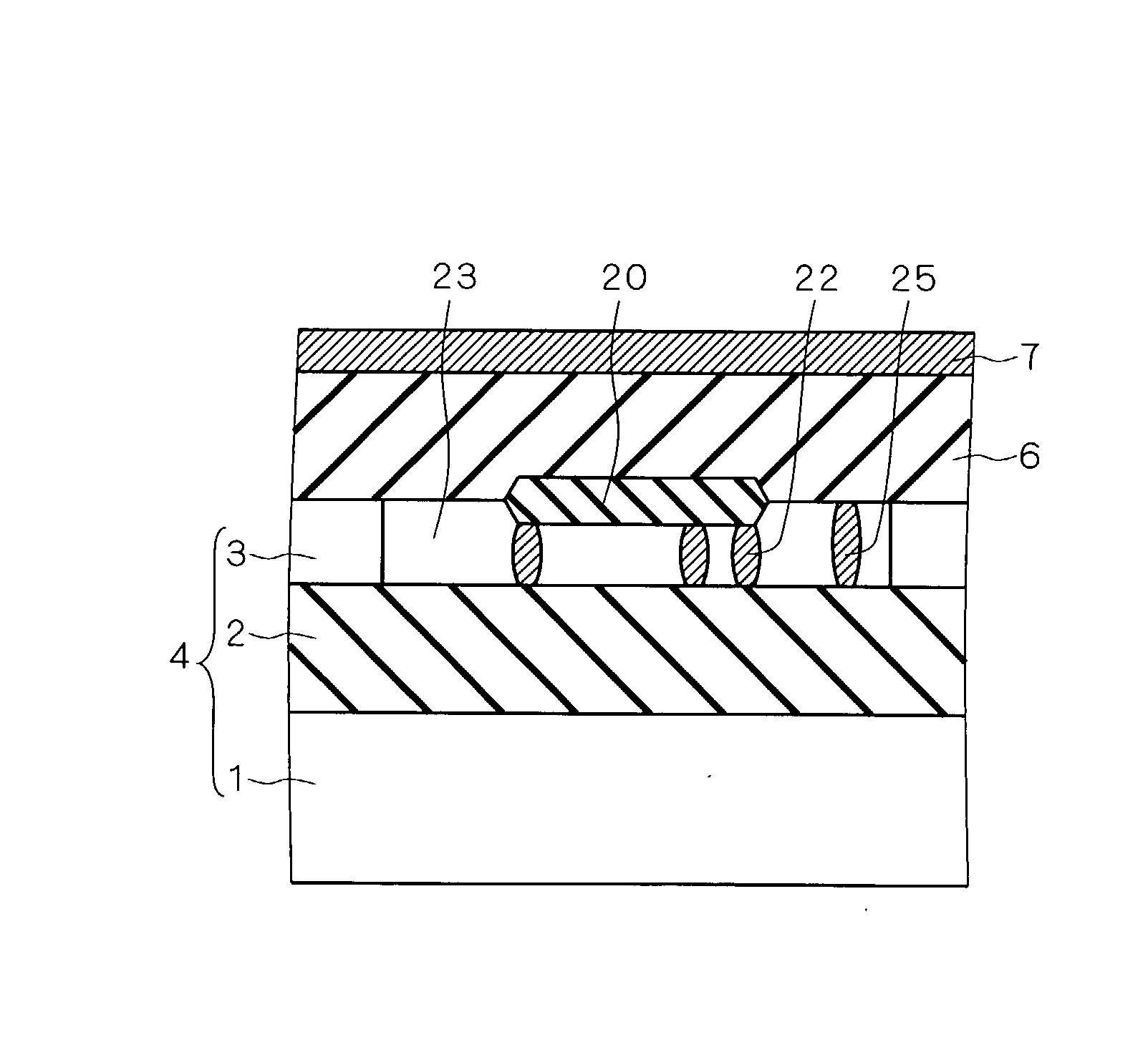
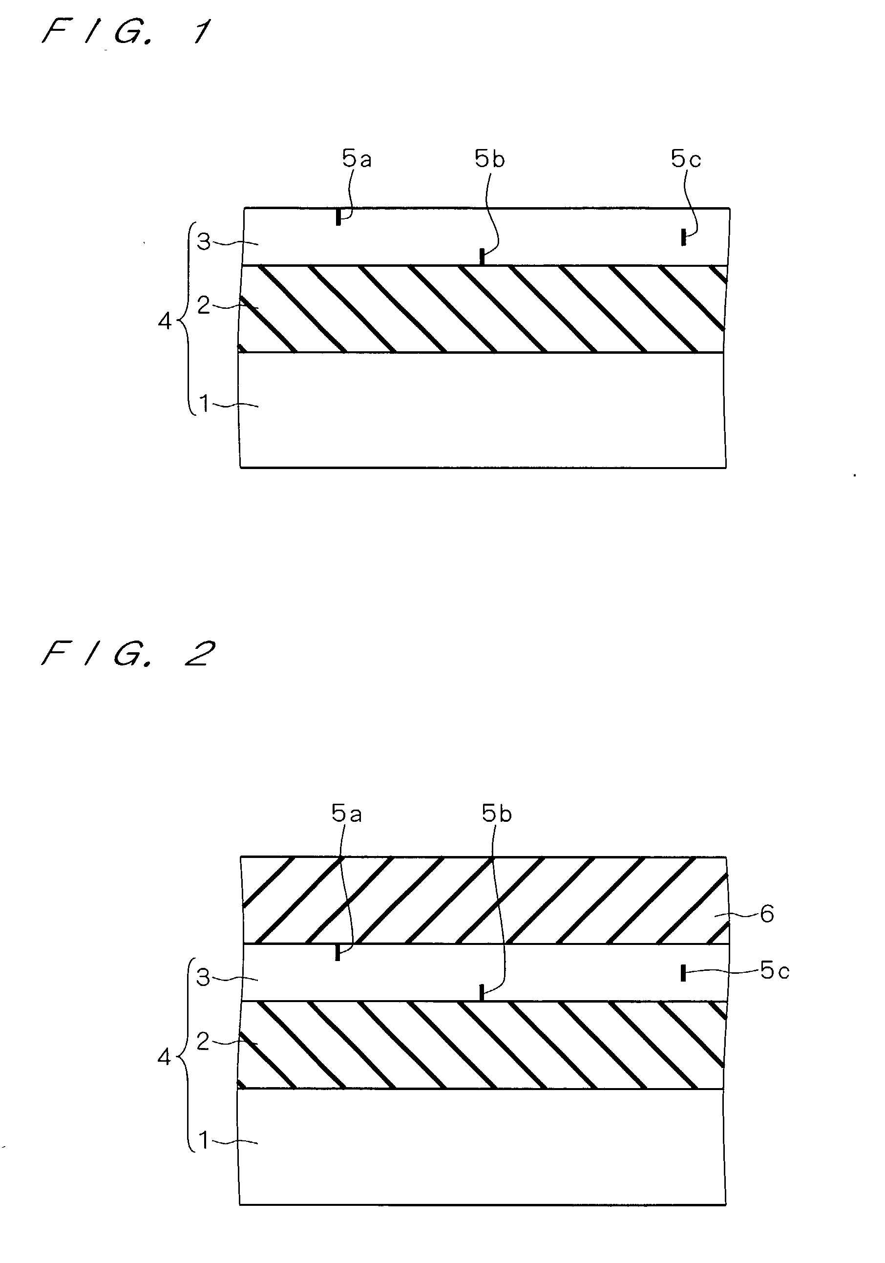
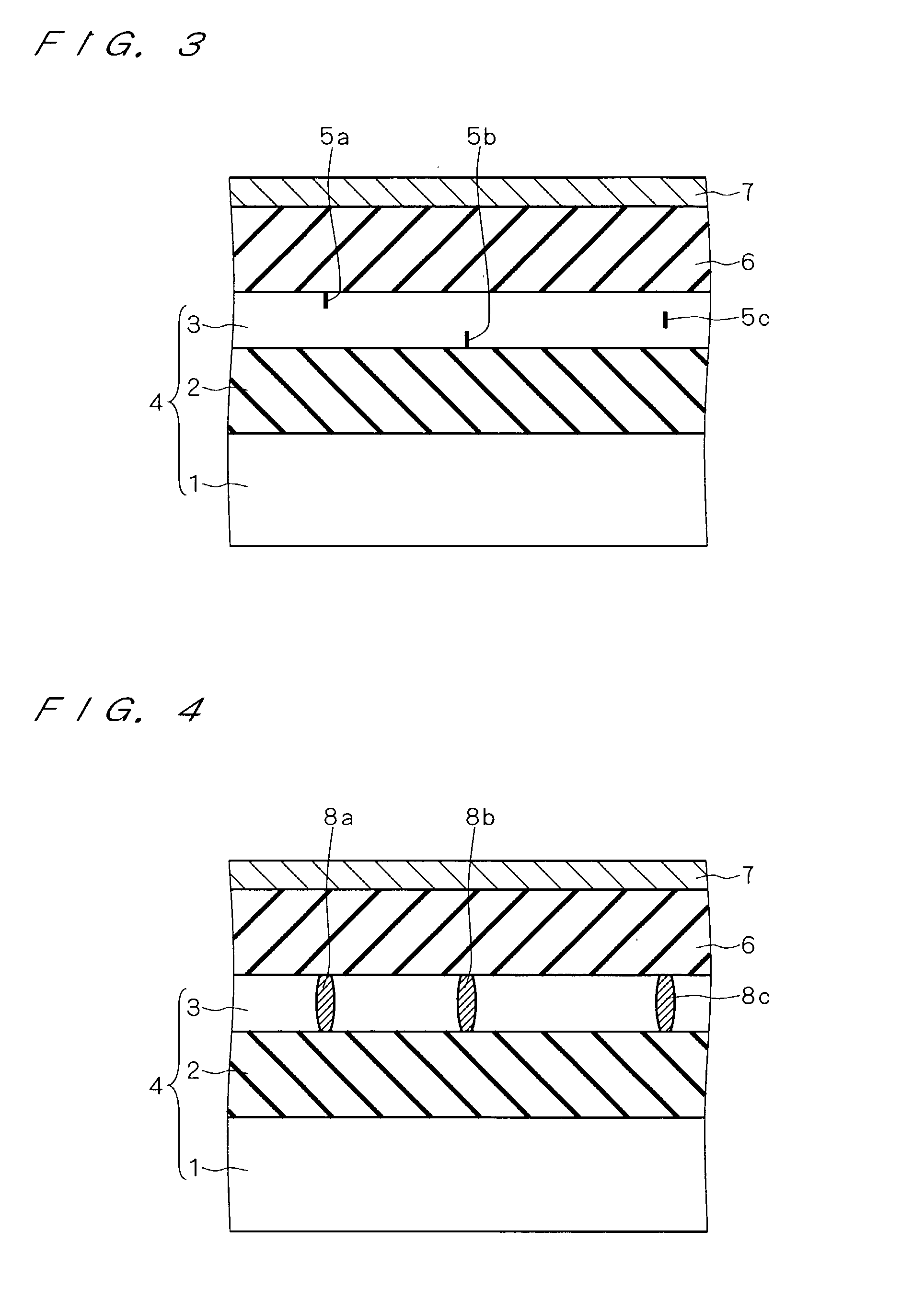
[0031] FIGS. 1 to 5 are sectional views of structures in the course of respective steps included in a method of evaluating a crystal defect according to a first preferred embodiment, for illustrating the method in order of occurrence of the respective steps. Referring to FIG. 1, first, an SOI substrate 4 which has a support substrate 1 of silicon, a buried oxide layer 2 made of a silicon oxide film and an 801 layer 3 of silicon which are stacked in this order is prepared. For the SOI layer 3, a thin film SOI layer having a film thickness of 100 nm or smaller can be employed. The SOI layer 3 contains crystal defects 5a to 5c generated during manufacture of the SOI substrate 4. The SOI layer 3 is a film to which evaluation of crystal defects is directed. Additionally, for the SOI substrate 4, a substrate having a structure in which a thin film surface layer (Si layer or a SiGe layer) with a film thickness of 100 nm or smaller is formed on a silicon substrate may alternatively b...


PUM


Abstract

In order to obtain a method of evaluating a crystal defect which allows crystal defects generated in a thin film SOI layer or a thin film surface layer to be evaluated using an in-line test, an SOI layer 3 has silicide regions 8 formed in the evaluation region consequently upon generation of crystal defects generated in the SOI layer 3. The silicide regions 8 are regions silicided as a result of the crystal defects having gettered metals which are contained in a transition layer 10 and diffuse into the SOI layer 3 upon a heat treatment. A laser beam is irradiated to the evaluation region via the transition layer 10 and the silicon oxide film 6. By monitoring a current flowing between first and second probes using an ampere meter while scanning the evaluation region with a laser beam, it is possible to evaluate the crystal defects in the evaluation region.

Description

[0001] 1. Field of the Invention[0002] The present invention relates to a method of detecting a crystal defect, a method of manufacturing a semiconductor device for evaluation, a method of evaluating a crystal defect and a semiconductor device for evaluation, which are used to evaluate a crystal defect generated within a semiconductor layer.[0003] 2. Description of the Background Art[0004] Crystal defects which are likely to occur during manufacture of a semiconductor substrate, or are induced in a semiconductor substrate due to a manufacturing process for a semiconductor device, cause degradation of various device characteristics such as junction characteristics (i.e., increase in junction leakage), on one hand. On the other hand, however, crystal defects, provided that the density or location thereof is controlled, are utilized as gettering sites for removing metals contained in a region where a device is to be formed. For this reason, quantitative evaluation of crystal defects ge...

Claims


Application Information

Patent Timeline
IPC IPC(8): H01L23/544H01L21/66
CPCH01L22/34H01L22/00
Inventor NARUOKA, HIDEKI
Owner RENESAS TECH CORP
Why Eureka
Try Eureka