
Thin film filters having a negative temperature drift coefficient and method making the same

a technology of temperature drift coefficient and thin film, applied in the field of thin film filters, can solve the problems of increasing the probability of damage to the film stack during cutting, increasing the internal stress of the film stack, and peeling of the film stack from the substrate, so as to promote the narrowing of the pass bandwidth

Inactive Publication Date: 2003-07-10
GOOGLE LLC
View PDF4 Cites 14 Cited by
  • Summary
  • Abstract
  • Description
  • Claims
  • Application Information

AI Technical Summary

Benefits of technology

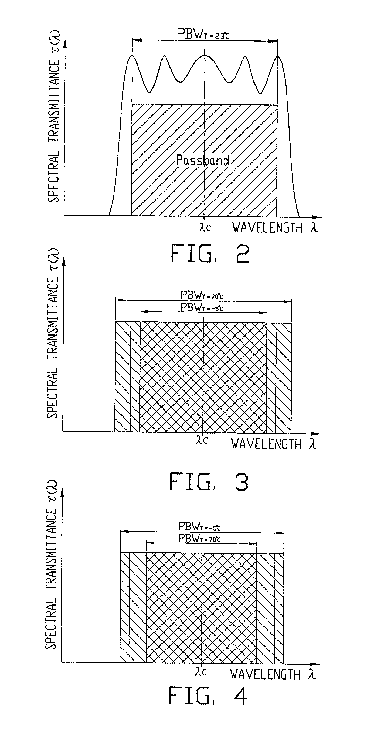
[0009] An object of the present invention is to provide thin film filters having a negative temperature drift coefficient and the method making the same, thus promoting a narrowing of pass bandwidth as temperature rises within its operational temperature range.

Problems solved by technology

However, this procedure inevitably induces more internal stress in the film stack.
The tensile stress endured by the film stack is also a disadvantage during cutting operations, since it makes the affected film layers more brittle, increasing the probability of damage to the film stack during cutting.
Furthermore, the adhesion between the film stack and the substrate maybe overstressed, resulting in peeling of the film stack from the substrate.

Method used


Image

  • Thin film filters having a negative temperature drift coefficient and method making the same
  • Thin film filters having a negative temperature drift coefficient and method making the same
  • Thin film filters having a negative temperature drift coefficient and method making the same

Examples


Embodiment Construction

[0019] The present invention provides two embodiments of a method for making thin film filters having a negative temperature drift coefficient.

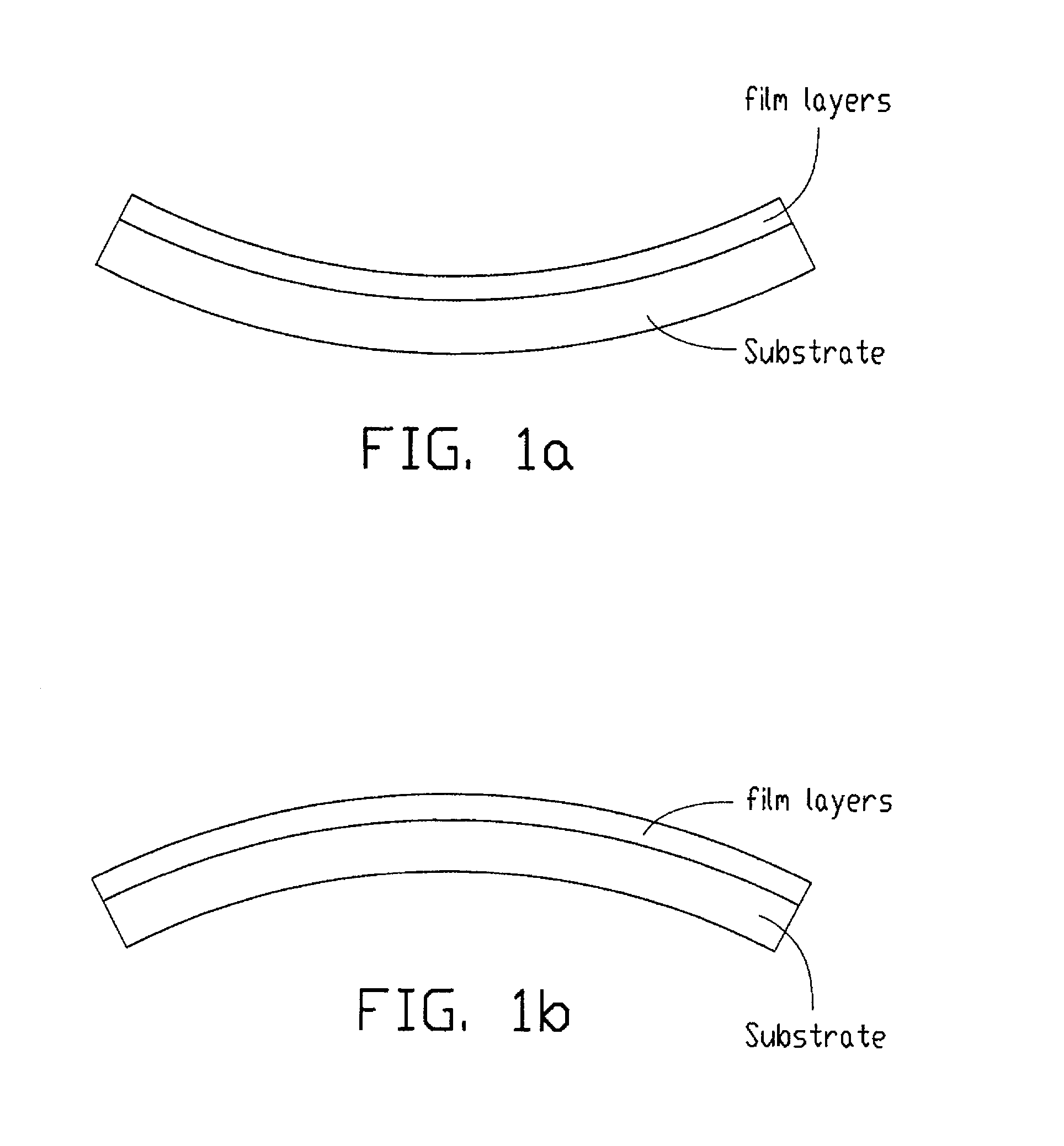
[0020] The first preferred embodiment of the present invented method for making thin film filters having a negative temperature drift coefficient generally comprises five steps as follows: 1. providing a substrate wafer which has a coefficient of thermal expansion (CTE) greater than that of selected film stack material; 2. polishing the substrate wafer; 3. depositing a stack of films each having a CTE smaller than that of the substrate wafer onto the substrate at a temperature substantially higher than room temperature; 4. cooling the resulting substrate-film laminate to room temperature, thus forming a convex-shaped substrate-film laminate; 5. cutting the cooled substrate-film laminate into pieces.

[0021] In the first step, a substrate wafer that has a CTE ranging from 10.times.10.sup.-6 / .degree. K to 20.times.10.sup.-6 / .degree. K is provided...


PUM

PropertyMeasurementUnit
wavelengthaaaaaaaaaa
roughnessaaaaaaaaaa

Abstract

Methods for making thin film filters having a negative temperature drift coefficient are the subject of the present invention. Such filters can achieve better optical control within an operational temperature range from -5 to 70 degrees centigrade. A first embodiment of the present invention includes the steps of: 1. providing a substrate wafer which has a coefficient of thermal expansion (CTE) greater than that of a selected film stack material; 2. polishing the substrate wafer; 3. depositing thin film layers made of the film stack material on the substrate wafer at a temperature substantially higher than room temperature; 4. cooling the substrate-film stack laminate to room temperature, thus forming a convex-shaped laminate; 5. cutting the cooled laminate into pieces. A second embodiment includes the steps of: 1. providing a laminate compose of a glass substrate and a film stack; 2. using at least one ion beam source to bombard the film stack of the laminate with high energy ions; 3. cutting the bombarded laminate into pieces.

Description

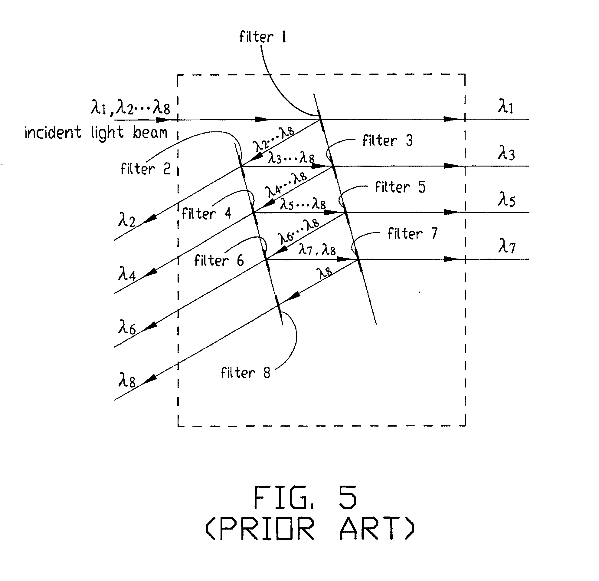
[0001] 1. Field of the Invention[0002] The present invention relates to thin film filters and the method making the same, and particularly to thin film filters having a negative temperature drift coefficient which can achieve better control of the optical performance of a DWDM system when working within the operational temperature range. The related invention record was filed in PTO with disclosure document no. 495113 on Jun. 12, 2001.[0003] 2. Description of Related Art[0004] In recent years, thin film filters have often been used in optical systems for signal processing or optical communications. The filters operate to select light of desired wavelengths, often within a narrow band. Thin film filters may be used in association with gradient refractive index (GRIN) lenses and optical fibers to form a dense wavelength division multiplexing (DWDM) device. Referring to FIG. 5, the operating principle of an eight-channel, filter type DWDM device is illustrated. Ideally, a light beam of...

Claims


Application Information

Patent Timeline
Patent Type & Authority Applications(United States)
IPC IPC(8): C03C17/34G02B1/12G02B5/28G02B7/00
CPCC03C17/3417C03C2218/32G02B1/12Y10T428/12611G02B7/008Y10T428/12618Y10T428/12535G02B5/285
Inventor CHEN, GA LANELEU, CHARLES
Owner GOOGLE LLC
Learn More