Packaging and alignment methods for optical components, and optical apparatus employing same

a technology of optical components and alignment methods, applied in the field of packaging and alignment methods for optical components, can solve the problems of low cumbersome and slow fully active fiber alignment process embodied in the standard procedure, and inability to meet the needs of high volume, high yield and low cost manufacturing,

Inactive Publication Date: 2003-07-17
WAGNER DAVID K +4
View PDF0 Cites 25 Cited by
  • Summary
  • Abstract
  • Description
  • Claims
  • Application Information

AI Technical Summary

Benefits of technology

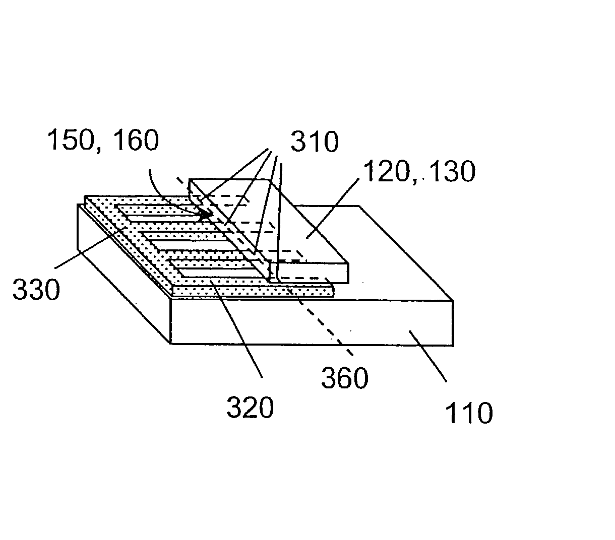
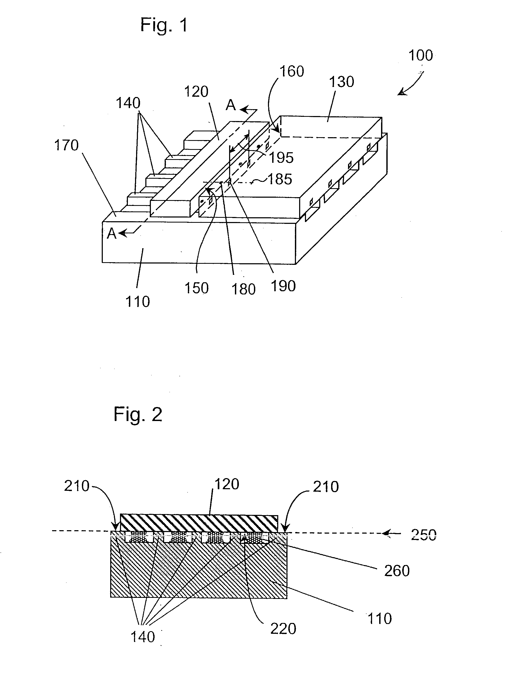
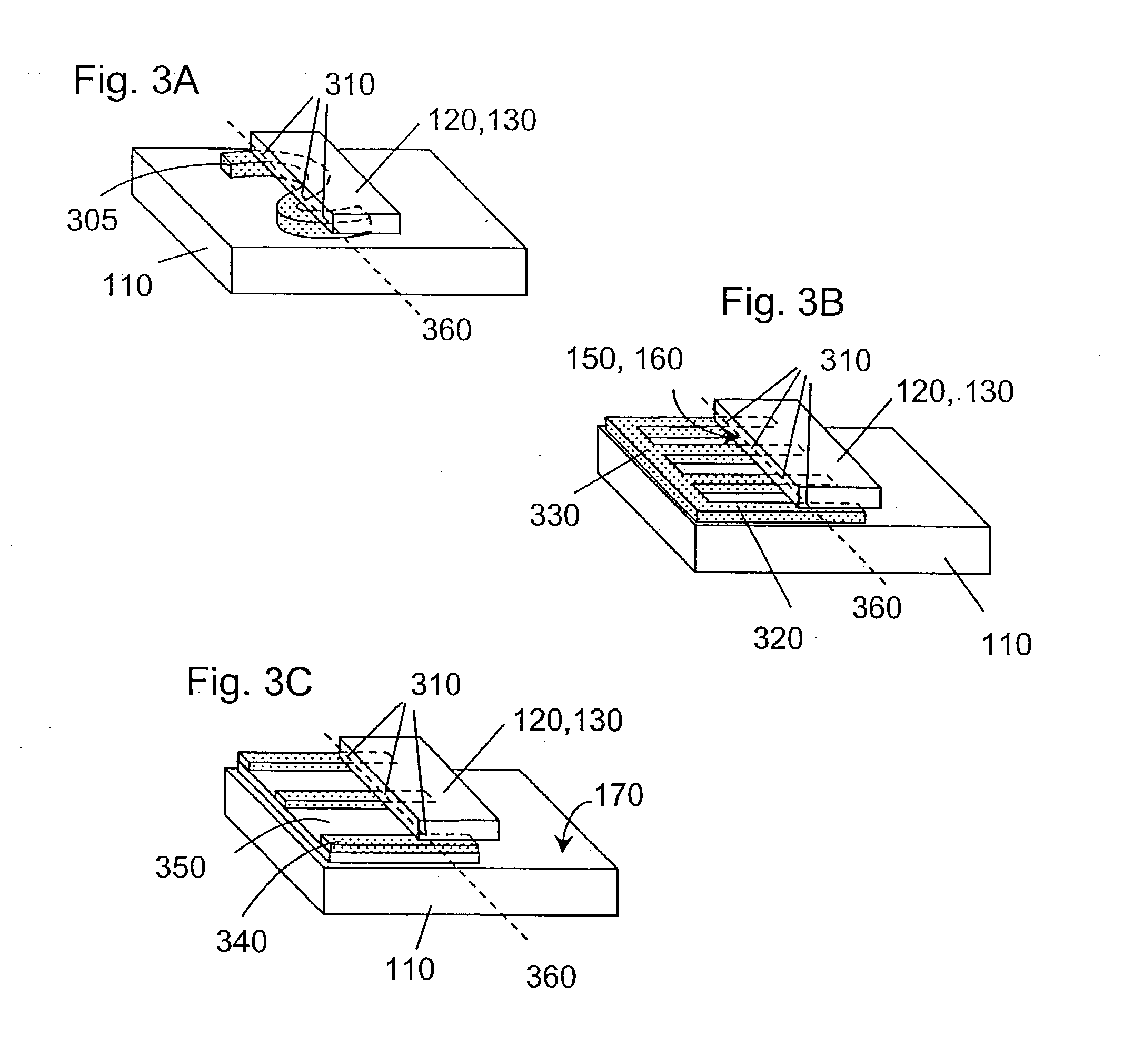
[0012] The effectiveness of this technique permits the optical component to be an optical array component such as a laser diode array, a photodetector array, an integrated optical chip, or an optical fiber array, but the techniques can also be used with components having only a single optical port. If the optical component is to be aligned with a second optical component, then the second optical component can be attached to the submount in the same manner. Thus vertical alignment can be achieved simply, inexpensively and precisely between multiple ports of optical array components.
[0013] The use of a standoff structure, which preferably has a total surface area contacting the optical components which is smaller, preferably much smaller, than the area by which the optical components overlap the submount, can substantially reduce the probability that alignment will be degraded by a foreign particle becoming lodged between the standoff structure and the optical component. Although not essential, it is advantageous for optimum vertical alignment and minimum curvature of the optical component along the emitting or receiving edge thereof, if the standoff structure includes at least three consecutive contact portions disposed along a straight line parallel to the subject edge of the optical component, mutually isolated from each other along that straight line.

Problems solved by technology

The fully active fiber alignment process embodied by the standard procedure is both cumbersome and slow, and although it can provide remarkably good coupling efficiency between the diode laser and fiber (in excess of 60%) it does not lend itself well to high volume, high yield and low cost manufacturing.
As a further limitation, the foregoing procedure has been used only for single-emitter individual LD geometries, and consequently mounting fixtures and handling apparatus used to adjust the fiber position are limited to single fibers and single-emitter LDs.
A major shortcoming of prior packaging techniques utilizing passive or semi-passive alignment of optical components is that such techniques generally cannot provide a sufficiently high degree of alignment precision.
In particular, it is difficult or impossible to simultaneously achieve highly precise vertical alignment (alignment in the direction perpendicular to the major plane of the components) in each optical channel between multi-channel components, such as an LD emitter array and an integrated optics chip, due to (inter alia) solder thickness and bonding pressure variations across the lateral dimension of the components.
Problems with misalignment in the vertical direction may be exacerbated by the occurrence of warping, bowing, curling or other planar nonuniformities in the components to be aligned, and / or by the presence of foreign particles between on or both of the components and the submount.
The failure of prior art techniques to effect precise and uniform vertical alignment between corresponding channels of multi-channel optical components results in high and non-uniform coupling losses, thereby limiting the usefulness of devices manufactured such techniques.
Many types of optoelectronic and integrated optics chips are known to exhibit nonplanarities such as warping, curling, and bowing that can easily exceed the allowable coupling alignment tolerance.
Such nonplanarities may result from stresses developed during various processing steps.
Maintaining this degree of parallelism as the submount and chuck are heated to melt the bonding agent (for example, solder) and brought into contact proves to be outside the capabilities of current state-of-the-art bonding equipment.
It is observed that even if the array component and submount can at first be angularly aligned with the required accuracy, thermal expansion and mechanical misalignments during the approach to contact generally result in misalignment at the moment of contact.
This variation cannot be predicted as it depends on the mechanical and thermal variations of the apparatus, which are not necessarily uniform or repeatable.
In addition, if the optical array component is warped, curled or bowed, it will be apparent that use of a rigid chuck would result in contact being made with one point on the optical component before any other, hence resulting is a substantially non-uniform distance between the reference surface defined by the standoff structure and the vertical positioning of the optical ports in the optical array component.
However optoelectronic components such as LD arrays or bars are generally narrow and fragile and thus would be subject to excessive force and consequent damage, especially at the peripheral corners which have the all important optical ports, and where any damage is fatal to device performance.
In addition, such chucks are generally designed simply to ensure that all solder contact pads make contact with rather large solder balls, so that there are no defects in the electrical connection to the component being bonded, and are not designed to provide co-planarization with sub-micron accuracy over millimeters of component width as required for IO packaging.

Method used


Image

  • Packaging and alignment methods for optical components, and optical apparatus employing same
  • Packaging and alignment methods for optical components, and optical apparatus employing same
  • Packaging and alignment methods for optical components, and optical apparatus employing same

Examples


Embodiment Construction

and Method

[0072] Referring to FIGS. 10 and 11, there is shown a preferred array device 1000 comprising a single crystal silicon submount 1010, a diode laser array chip 1020 herein called a laser bar, and a lithium niobate waveguide array chip 1030 herein called a LN WG chip, constructed according to the method of this invention. The laser bar 1020 in this example is 10 mm wide as measured in the direction indicated by the arrows labeled C in FIG. 10, 0.5 mm long, and 0.1 mm thick, and contains around 100 individual diode lasers also called stripes or emitters. A standoff structure 1040, comprising a series of parallel, longitudinally oriented rib standoffs, is shown on the surface of the submount 1010. The upper surfaces of the standoffs define a reference surface 1150. The standoffs are fabricated by photolithography and etching, using one of the standard processes employed in silicon wafer fabrication. The height 1142 of the standoff structures is around 0.005 mm, and their width ...


PUM


Abstract

Roughly described, a submount has a standoff structure protruding from its surface. An optical component is pressed against the standoff structure until tilt and planar non-uniformities are removed, and then bonded to the submount using an adhesive placed in the wells between the protrusions of the standoff structure. The standoff structure preferably has a total surface area contacting the optical component which is much smaller than the area by which the optical components overlap the submount. The optical component mounted in this manner can be an optical array component (including an optical fiber array), or a component having only a single optical port. A second optical component can be attached to the submount in the same manner, greatly simplifying the vertical alignment problems between the two components.

Description

[0001] 1. Field of the Invention[0002] The invention relates generally to packaging of optical and optoelectronic components, and more specifically to techniques for optical alignment and attachment of planar and planar array optical waveguides.[0003] 2. Description of Related Art[0004] In the manufacturing of optoelectronic and lightwave systems, optical alignment is an important requirement beyond the electrical contact, mechanical support, and reliability requirements existing for electronic packaging. Alignment of different devices and chips, such as micron-scale laser diodes (herein abbreviated as LDs), electro-optic devices, single mode fibers, and other optical waveguiding structures, is necessary because not all useful functionalities in the current art can be obtained in the same substrate material. Thus the type of packaging where it is necessary to couple optical energy between waveguiding structures in and on different chips and substrates (herein called "integrated opti...

Claims


Application Information

Patent Timeline
Patent Type & Authority Applications(United States)
IPC IPC(8): G02B6/42H01S3/0941H01S5/00H01S5/40
CPCG02B6/422G02B6/4226G02B6/4227H01S5/4025H01S3/0941H01S5/005G02B6/423G02B6/4242G02B6/4244G02B6/4245
Inventor WAGNER, DAVID K.GUENTHER, HARALDBISCHEL, WILLIAM K.LI, JIM WEIJIANMOROZOVA, NINA D.
Owner WAGNER DAVID K
Why Eureka
Try Eureka