Heterojunction bipolar transistor and semiconductor integrated circuit device using the same

a technology of integrated circuits and transistors, applied in the direction of semiconductor devices, electrical equipment, basic electric elements, etc., can solve the problems of avalanche breakdown, low breakdown voltage, and high-frequency characteristics of transistors

Inactive Publication Date: 2003-07-24
RENESAS ELECTRONICS CORP
View PDF0 Cites 29 Cited by
  • Summary
  • Abstract
  • Description
  • Claims
  • Application Information

AI Technical Summary

Problems solved by technology

If so, the high-frequency characteristics of the transistor will deteriorate because of the accumulation and retention effect of carriers caused by the conduction band discontinuity.
However, the above-described prior-art energy band structures shown in FIGS. 2 to 4 have the following problems.
As a result, a problem that the breakdown voltage decreases arises.
As a result, there arises a problem that avalanche breakdown is likely to occur in the layer 116a.
This means that the breakdown voltage is likely to lower.
Moreover, even if the band gap discontinuity is apparently relaxed, this is unable to be really eliminated.
Thus, the energy band structure of FIG. 3 is unnecessary.
However, if so, there arises a problem of degradation of the rising characteristic of the collector current-collector voltage characteristic.
As a result, there arises aproblem of degradation of the rising characteristic of the collector current-collector voltage characteristic, as well.

Method used


Image

  • Heterojunction bipolar transistor and semiconductor integrated circuit device using the same
  • Heterojunction bipolar transistor and semiconductor integrated circuit device using the same
  • Heterojunction bipolar transistor and semiconductor integrated circuit device using the same

Examples


first embodiment

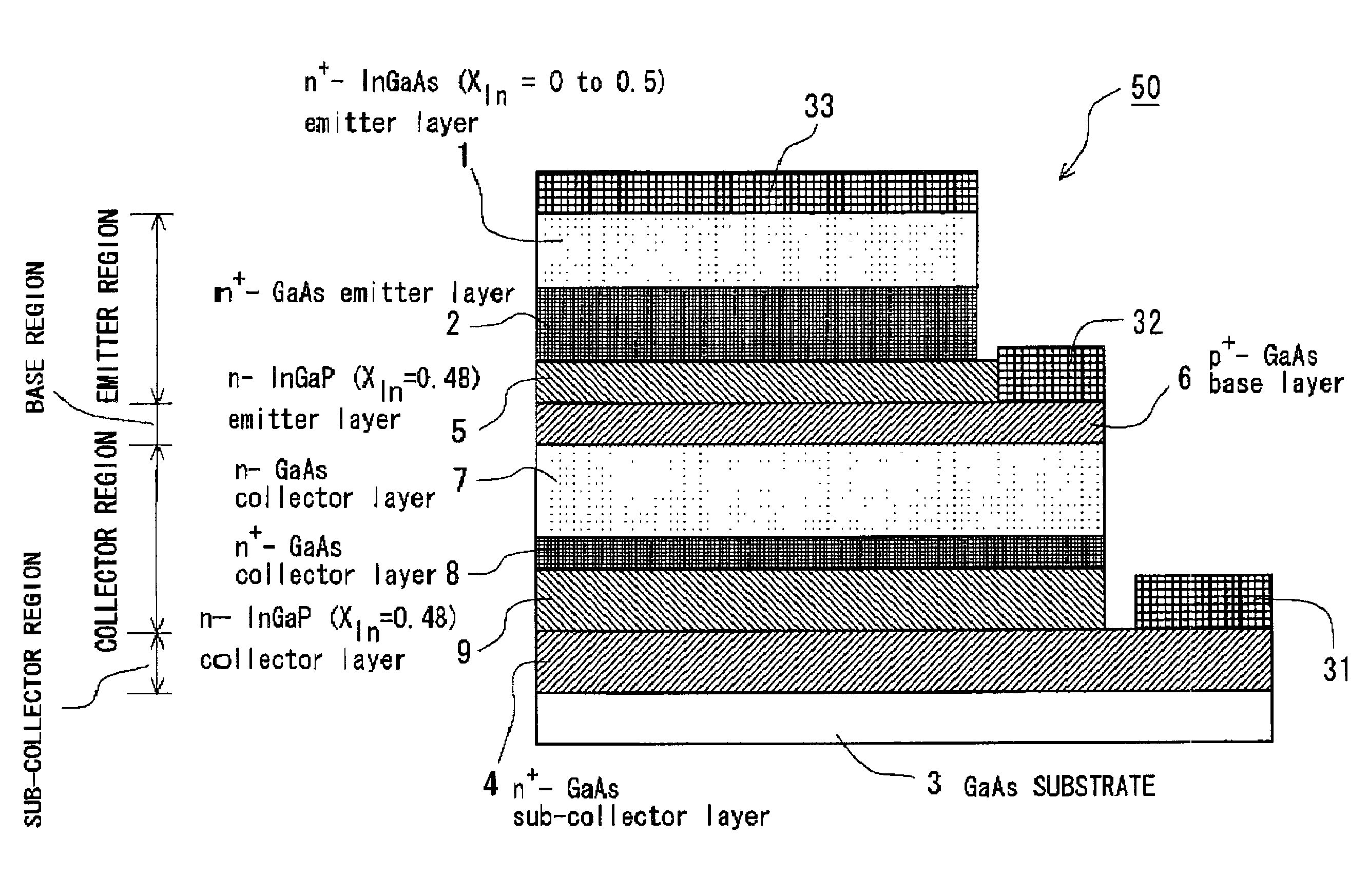
[0056] FIG. 5 shows the layered structure of a npn-type heterojunction bipolar transistor 50 according to a first embodiment of the invention.

[0057] As shown in FIG. 5, the transistor 50 comprises a semi-insulating GaAs substrate 3, a n.sup.+-type GaAs sub-collector layer 4 (thickness: 500 nm) formed on the substrate 3, and a n-type InGaP collector layer 9 (thickness: 100 nm) formed on the layer 4. The surface of the sub-collector layer 4 is partially exposed from the overlying collector layer 9. A collector electrode 31 is formed on the exposed part of the layer 4.

[0058] The n.sup.+-type GaAs sub-collector layer 4 is doped with silicon (Si) as a n-type dopant at a doping concentration of 4.0.times.10.sup.18 cm.sup.-3. The n-type InGaP collector layer 9 has a composition ratio of In (i.e., X.sub.In) of 0.48 and thus, it is expressed as In.sub.0.48Ga.sub.0.52P. However, the In composition ratio X.sub.In may be set at a value in the range from 0.48 to 0.5. The n.sup.+-type InGaP colle...

second embodiment

[0090] FIG. 11 shows the layered structure of a npn-type heterojunction bipolar transistor 50A according to a second embodiment of the invention.

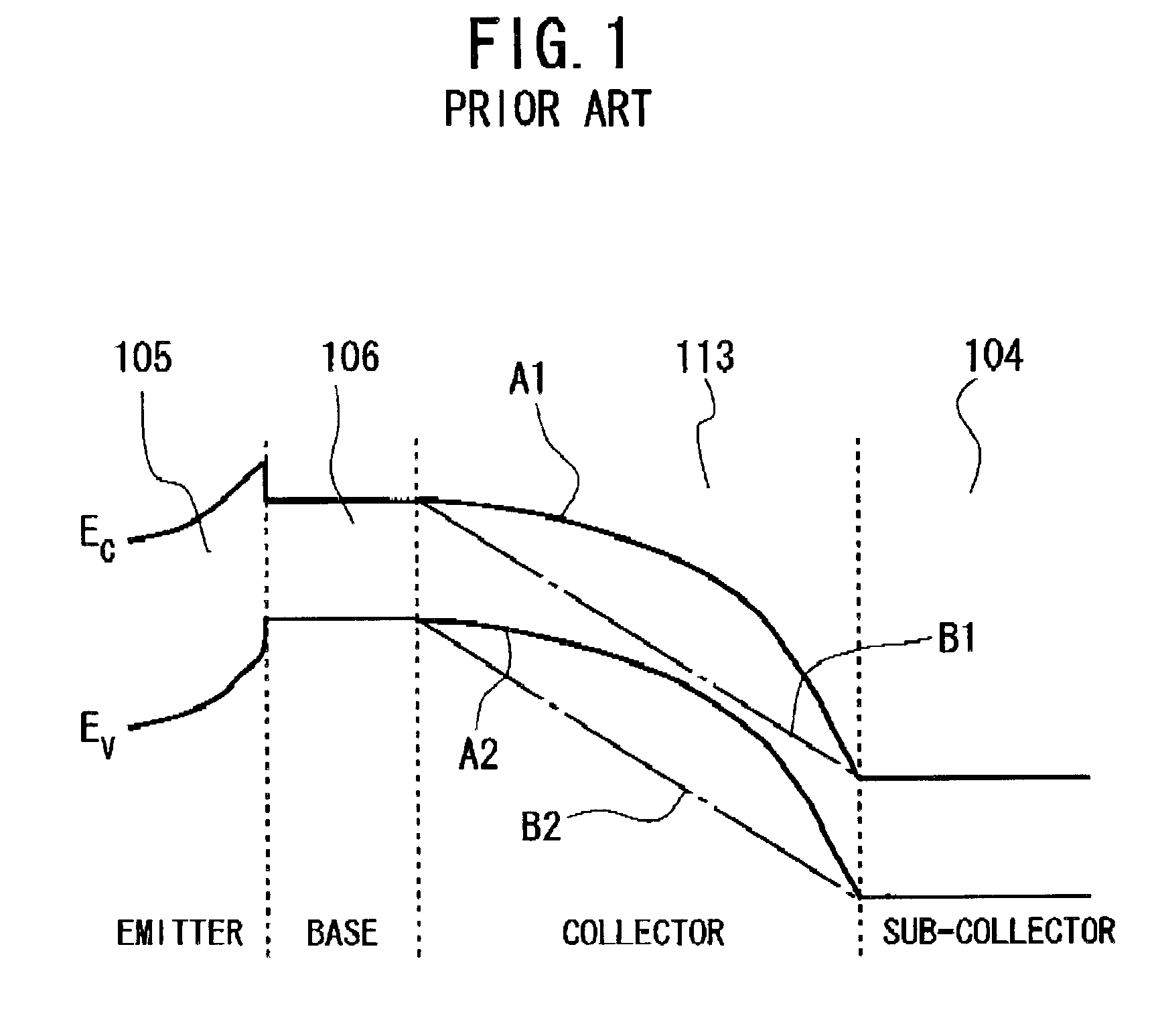
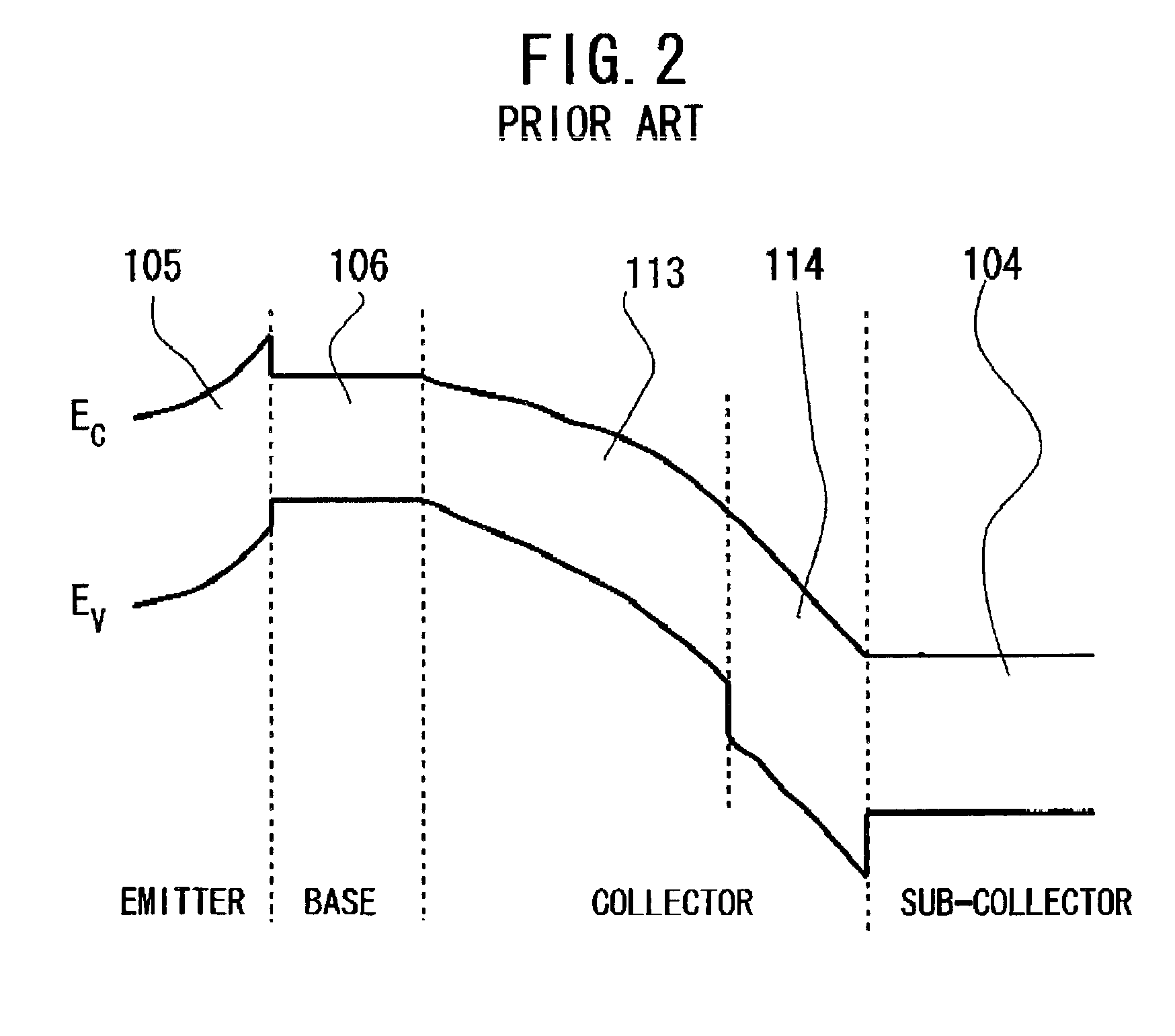
[0091] With the above-described heterojunction bipolar transistor 50 according to the first embodiment of FIG. 5, the high-electric field part is generated in the n.sup.+-type InGaP collector layer 9. However, if the doping concentration of the n.sup.+-type GaAs sub-collector layer 4 is insufficient, the depletion layer formed in the collector region (i.e., in the collector layers 7, 8, and 9) will expand to the inside of the sub-collector layer 4. In this case, high electric field will be generated in the depleted part of the layer 4. Accordingly, to make sure that the advantages of the invention are obtainable, it is preferred that a semiconductor layer having a wider energy band gap than the collector layer 7 is additionally provided on the side of the sub-collector layer 4 to be adjacent to the collector layer 9. The transistor 50A of t...

third embodiment

[0098] FIG. 12 shows the circuit diagram of a semiconductor integrated circuit device (IC) 60 according to a third embodiment of the invention. This IC or device 60 is applicable to high-output amplifier IC for microwaves.

[0099] As shown in FIG. 12, the IC 60 comprises an amplifier 17aand an amplifier 17b serially connected to each other by way of an impedance-matching circuit 18 located therebetween. These elements 17a, 17b and 18 are located between a RF (Radio-Frequency) input terminal 19 and a RF output terminal 20. A bias circuit 21 supplies specific bias voltages to the amplifiers 17a and 17b.

[0100] The amplifier 17a, which is located on the input terminal side, is in a driver amplifier stage. The amplifier 17a comprises a plurality of the heterojunction bipolar transistors 50 or 50A according to the first or second embodiment, where the total emitter area of the transistors 50 or 50A used is set at 960 .mu.m.sup.2. The amplifier 17b, which is located on the output terminal si...


PUM


Abstract

A heterojunction bipolar transistor has a raised breakdown voltage and restrains the rising characteristic of IC-VCE characteristic from degrading. The collector region includes first, second, and third collector layers of semiconductor. The first collector layer is made of a doped or undoped semiconductor in such a way as to contact the sub-collector region. The second collector layer is made of a doped or undoped semiconductor having a narrower band gap than the first collector layer in such a way as to contact the base region. The third collector layer has a higher doping concentration than the second collector layer in such a way as to be located between or sandwiched by the first collector layer and the second collector layer.

Description

[0001] 1. Field of the Invention[0002] The present invention relates generally to heterojunction semiconductor devices. More particularly, the invention relates to a heterojunction bipolar transistor having a raised or improved breakdown (withstand) voltage, and a semiconductor integrated circuit device using the same.[0003] 2. Description of the Related Art[0004] To improve the collector-to-emitter breakdown voltage of heterojunction bipolar transistors during operation, it is important to suppress or prevent the avalanche breakdown in the collector region. To realize this, an improved structure has been developed and disclosed, where a semiconductor layer having a low or small impact ionization coefficient is inserted into a high electric-field part of the collector region. This structure is disclosed in, for example, the Japanese Non-Examined Patent Publication No. 7-16172 published in 1995.[0005] FIG. 1 shows schematically the energy band diagram of a prior-art heterojunction bi...

Claims


Application Information

Patent Timeline
Patent Type & Authority Applications(United States)
IPC IPC(8): H01L21/331H01L29/08H01L29/737
CPCH01L29/7371H01L29/0821H01L29/737
Inventor NIWA, TAKAKISHIMAWAKI, HIDENORIAZUMA, KOJIKUROSAWA, NAOTO
Owner RENESAS ELECTRONICS CORP
Why Eureka
Try Eureka