Semiconductor integrated circuit device and delay-locked loop device

a technology of integrated circuit and delaylock, which is applied in the direction of pulse automatic control, static storage, instruments, etc., can solve the problems of increased power consumption, hazard or abnormal pulses, and difficulty in maintaining high timing precision, so as to prevent deviation in output timing and reduce power consumption

Inactive Publication Date: 2003-08-14
PS4 LUXCO SARL
View PDF4 Cites 48 Cited by
  • Summary
  • Abstract
  • Description
  • Claims
  • Application Information

AI Technical Summary

Benefits of technology

0050] Accordingly, it is an object of the present invention to provide a DLL and a semiconductor integrated circuit device of reduced power consumption suited for use in equipment that complies with DDR-II specifications.
0051] Another object

Problems solved by technology

This makes it difficult to maintain a high timing precision.
The result is an increase in power consumption.
If the tap is changed over at the timing at which the signal that prop

Method used


Image

  • Semiconductor integrated circuit device and delay-locked loop device
  • Semiconductor integrated circuit device and delay-locked loop device
  • Semiconductor integrated circuit device and delay-locked loop device

Examples


first embodiment

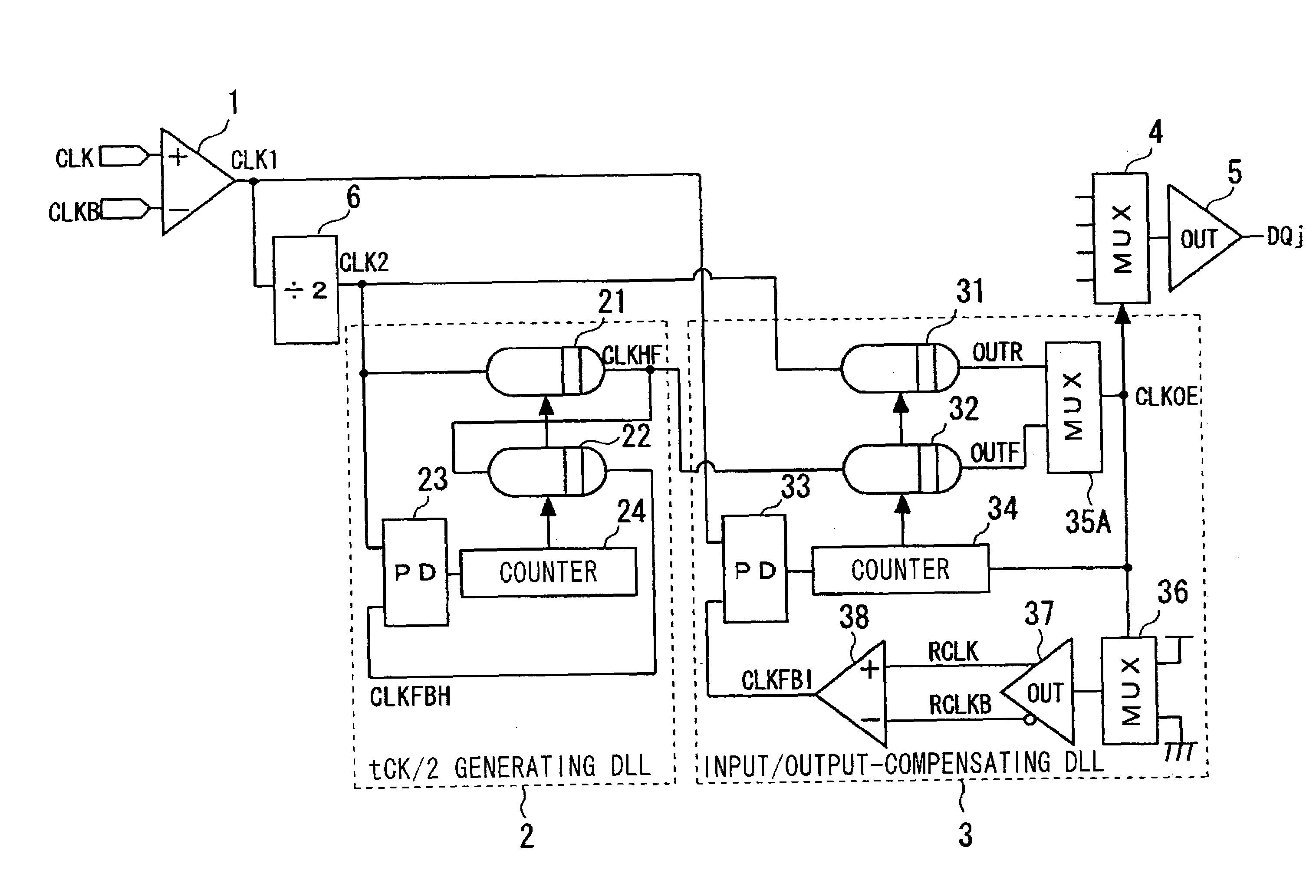
[0082] In the present invention, as shown in FIG. 1, a delay-locked loop (2) for a DCC function is so adapted that the delay times of serially connected first and second delay lines (21, 22) are adjusted in such a manner that a signal obtained by delaying an input signal by the first and second delay lines (21, 22) will be in phase with the input signal, as a result of which the first delay line (21) outputs a signal obtained by delaying the input signal by one half cycle of the input signal. The delay-locked loop (2) is provided with a frequency dividing circuit (6) for performing frequency-division of the input signal, and includes first delay adjusting means (23, 24) for delaying the output signal from the frequency dividing circuit (6) by the first and second delay lines (21, 22) and adjusting the delay times of the first and second delay lines (21, 22) in such a manner that the output signal of the frequency dividing circuit (6) and the output signal of the second delay line (2...

fourth embodiment

[0140] the present invention is as illustrated in FIG. 6 showing the structure thereof. This embodiment is obtained by providing the arrangement of FIG. 18 with the latch circuit (aligner) 39 for latching the tap selection signal from the counter 34.

[0141] The input / output-compensated DLL, here designated by a reference numeral 3", is so adapted that the aligner 39 latches the tap selection signal from the counter 34 at the output signal CLKOE of delay line 31.

[0142] A fifth embodiment of the present invention will now be described with reference to FIG. 7, which illustrates the structure of the fifth embodiment. As shown in FIG. 7, this embodiment is obtained by providing the tCK / 2 generating DLL 2" and a input / output-compensated DLL 3" in the arrangement of FIG. 1 having the frequency dividing circuit 6 with the latch circuits (aligners) 25 and 39, respectively, for latching the tap selection signals from the counters 24 and 34, respectively. Hazards do not occur at tap changeover...


PUM


Abstract

Disclosed are a delay-locked loop circuit and a semiconductor integrated circuit device of reduced power consumption, the delay-locked loop circuit having a tCK/2 generating DLL and an input/output-compensating DLL. The tCK/2 generating DLL includes first and second delay lines for delaying a frequency-divided clock input thereto from a frequency dividing circuit; a first phase detector for detecting the phase difference between the frequency-divided clock and the output of the second delay line; and a counter for outputting a signal that changes over the output taps of the first and second delay lines depending upon an output from the first phase detector. The input/output-compensating DLL includes third and fourth delay lines for delaying the frequency-divided clock input thereto; a multiplexer, to which output signals from the third and fourth delay lines are input, for outputting a signal in which timings of rising and falling edges are decided by rising edges of respective ones of the output signals and then by falling edges of respective ones of the output signals; a dummy multiplexer to which this output signal is input and having a delay time identical with that of a multiplexer that selects data; a dummy first buffer having a delay time identical with that of an output buffer; a dummy second buffer having a delay time identical with that of an input buffer; a second phase detector for detecting the phase difference between an output clock from the input buffer and the output of the dummy second buffer; and a counter for outputting a signal that changes over the output taps of the third and fourth delay lines depending upon an output from the second phase detector.

Description

[0001] This invention relates to a semiconductor integrated circuit device and, more particularly, to a delay-locked loop (DLL) and a semiconductor integrated circuit device equipped with the DLL.[0002] A DDR (Double Data Rate)-I-SDRAM (Synchronous Dynamic Random-Access Memory) is designed to perform data transfer at a transfer rate of 200 to 300 Mbps (megabits per second) with respect to an input clock having a frequency of 100 to 166 MHz. Design specification is such that data input is synchronized to both rising and falling edges of an input clock signal. The desired specifications can be achieved with a DLL of minimal structure by passing the entered clock through a single delay line as is.[0003] FIG. 18 is a diagram illustrating an example of a DLL(Delay Locked Loop) in compliance with DDR specifications, and FIG. 19 is a diagram illustrating the timing operation of this DLL.[0004] Referring to FIG. 18, the DLL 3A is equipped with an input buffer 1, the inputs to which are mutu...

Claims


Application Information

Patent Timeline
IPC IPC(8): G06F1/10G11C11/407G11C7/22G11C11/4076H03K5/00H03K5/13H03L7/08H03L7/081
CPCG11C7/1066G11C11/4076G11C7/222G11C7/22H03L7/08
Inventor TAKAI, YASUHIRO
Owner PS4 LUXCO SARL
Why Eureka
Try Eureka