Implantation for current confinement in nitride-based vertical optoelectronics

a technology of current confinement and vertical optoelectronics, which is applied in the direction of semiconductor lasers, semiconductor laser structural details, lasers, etc., to achieve the effect of reducing light absorption

Inactive Publication Date: 2003-09-25
RGT UNIV OF CALIFORNIA THE OFFICE OF TECH TRANSFER
View PDF8 Cites 48 Cited by
  • Summary
  • Abstract
  • Description
  • Claims
  • Application Information

AI Technical Summary

Benefits of technology

0015] The system according to the present invention includes a method for channeling the current through a low resistivity region such that carrier recombination takes place away from regions underneath the p-contact

Problems solved by technology

This leads to channeling, or confining, of the current through a low resistivity and unimplante

Method used


Image

  • Implantation for current confinement in nitride-based vertical optoelectronics
  • Implantation for current confinement in nitride-based vertical optoelectronics
  • Implantation for current confinement in nitride-based vertical optoelectronics

Examples


Embodiment Construction

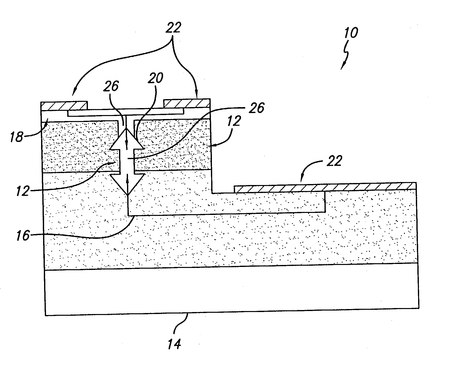
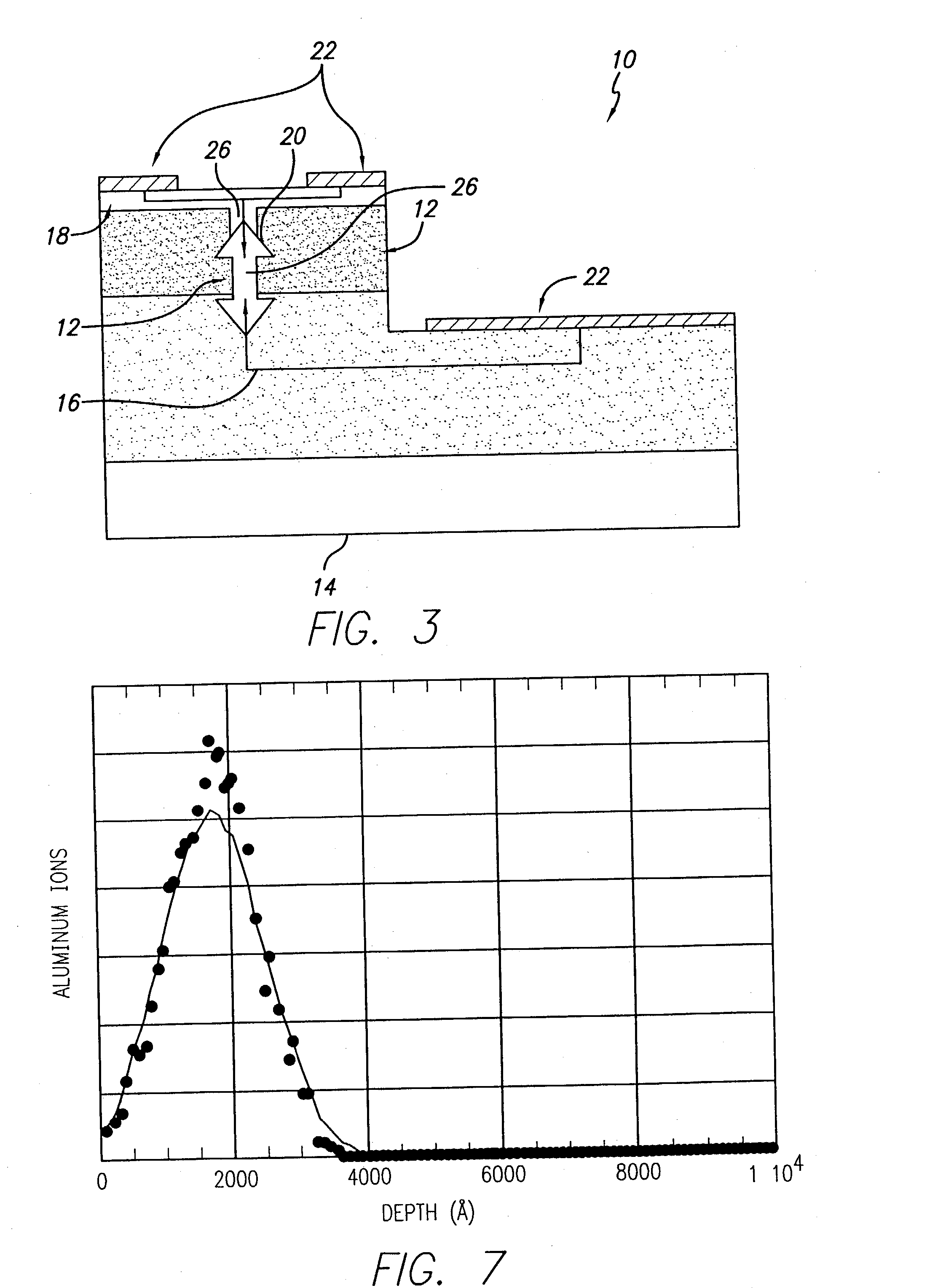
[0057] An LED structure with a 5000 .ANG. thick p-doped GaN top layer was implanted for current confinement.

[0058] (1) Using TRIM, for an aluminum species, an energy of 180 keV was chosen to disorder at least 1600 .ANG. of material (straggle and channeling in GaN will most likely increase this depth). The chosen dosage was 10.sup.14 cm.sup.-2.

[0059] (2) The sample was patterned with an alignment pattern made out of dielectric material (to survive the regrowth process; alternately, a refractory metal could be used).

[0060] (3) A 200 .ANG. / 2000 .ANG. Ti / Au mask was deposited using a liftoff process to serve as the implant mask. The titanium served as a metal-to-semiconductor sticking layer, and the gold thickness was chosen to exceed the penetration depth of 180 keV Al into Au calculated by TRIM simulations.

[0061] (4) The sample was then implanted at the above conditions.

[0062] (5) The metal mask was etched away (Au etchant and BHF).

[0063] (6) A 1200 .ANG. p-doped (Mg) GaN layer was re...


PUM


Abstract

Ion implantation is used to increase the resistivity of semiconductor device layers for channeling the current through a low resistivity, unimplanted region such that carrier recombination takes place away from regions underneath the contacts. This eliminates absorption of light by the contact thereby providing higher light output power and better current-voltage characteristics to the semiconductor device. The incorporation of a regrown contact layer allows for an undamaged lateral conduction path, and the fabrication of ohmic contacts.

Description

[0001] 1. Field of the Invention[0002] This invention pertains to the processing of semiconductor material in vertical opto-electronic devices.[0003] More specifically, the invention pertains to applying a series of processing steps to nitride based materials (e.g., GaN, InN, AIN, BN based materials) for improving the quality of the cavity, and consequently, the opto-electronic device performance.[0004] 2. General Background and State of the Art[0005] Recently, the demand for nitride based semiconductor materials (e.g., having Gallium Nitride or GaN) for opto-electronics has increased dramatically for applications such as video displays, optical storage, lighting, medical instruments, etc.. For many of these applications, vertical cavity structures (e.g., vertical cavity surface emitting lasers or VCSELs) offer advantages such as low-cost arrays and directional emission, in combination with a geometry that is easier to integrate into multi-device systems.[0006] At present, there hav...

Claims


Application Information

Patent Timeline
IPC IPC(8): H01L33/14H01S5/02H01S5/183H01S5/20H01S5/323H01S5/343
CPCB82Y20/00H01L33/145H01S5/0421H01S2304/12H01S5/2063H01S5/32341H01S5/34333H01S5/18308
Inventor MARGALITH, TALCOLDREN, LARRY A.NAKAMURA, SHUJI
Owner RGT UNIV OF CALIFORNIA THE OFFICE OF TECH TRANSFER
Why Eureka
Try Eureka